
Method for preparing ridge-shape light-wave-guide of optical crystal by ion injection method

An optical crystal and ion implantation technology, applied in the direction of optical waveguide light guide, optics, light guide, etc., can solve the problems that are difficult to realize, the influence of nonlinear optical properties of optical waveguide, etc., and achieve the effect of easy adjustment and control, and strong universality

Inactive Publication Date: 2003-08-27
SHANDONG UNIV
View PDF0 Cites 17 Cited by
  • Summary
  • Abstract
  • Description
  • Claims
  • Application Information

AI Technical Summary

Problems solved by technology

In 1992, the American scientific journal "Electronics Letter" published a SiGe / Si ridge optical waveguide (Y.M.Liu, et al, 28 (1992) 1434) using selective etching to form a silicon substrate; in the same year, it was published in the same magazine Ridge-shaped optical waveguides are formed by Ge diffusion on silicon-based substrates (S.F.Pesarcik, et al., E28 (1992) 159), and the formation of strip-shaped optical waveguides, especially ridge-shaped optical waveguides, mainly consists of ion exchange and high-temperature diffusion Anisotropic etching on the formed planar optical waveguide, or chemical vapor deposition or molecular beam epitaxy on the substrate using a mask, these methods are mostly chemical processes, and the nonlinear optical properties of the prepared optical waveguide are affected; These methods are material-specific and difficult to implement on other optical crystal materials

Method used


Image

  • Method for preparing ridge-shape light-wave-guide of optical crystal by ion injection method
  • Method for preparing ridge-shape light-wave-guide of optical crystal by ion injection method
  • Method for preparing ridge-shape light-wave-guide of optical crystal by ion injection method

Examples


Embodiment 1

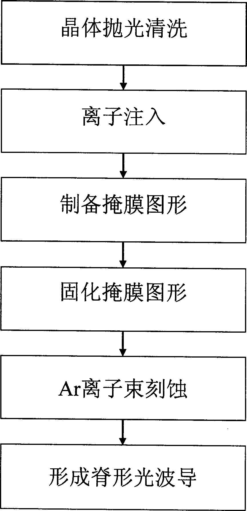
[0017] (5) Specific implementation methods Example 1: Preparation of ridge-shaped optical waveguide with increased refractive index of barium metaborate (β-BBO) crystal

[0018] Sample polishing: Cut the β-BBO crystal as a Z-cut with a size of 10 mm × 7 mm and a thickness of 2 mm, and the surface is optically polished. After the optical crystal (1) is cleaned with neutral detergent, deionized water and absolute ethanol, it is ready for ion implantation.

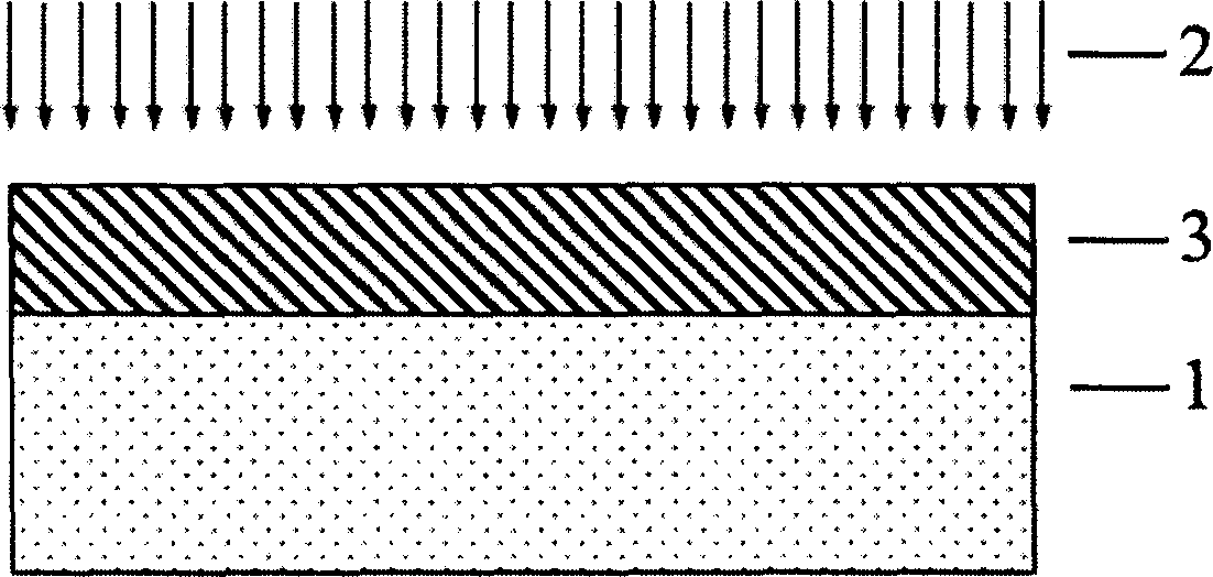
[0019] Ion implantation: put the prepared bottom sample in the target chamber of the accelerator, and evacuate to 10 -4 Pascal (Pa) magnitude. MeV energy ion implantation (2), the implantation conditions are: implanted ions: oxygen ions (O + ), ion energy: 2.2 megaelectric volts (MeV), implant dose: 5.0×10 14 ions / cm2. The ion beam current was 60 nanoamperes and the scanning area was 15 cm x 20 cm. Under this condition, a planar optical waveguide (3) with increased anomalous light refractive index in the waveguide region...


PUM


Abstract

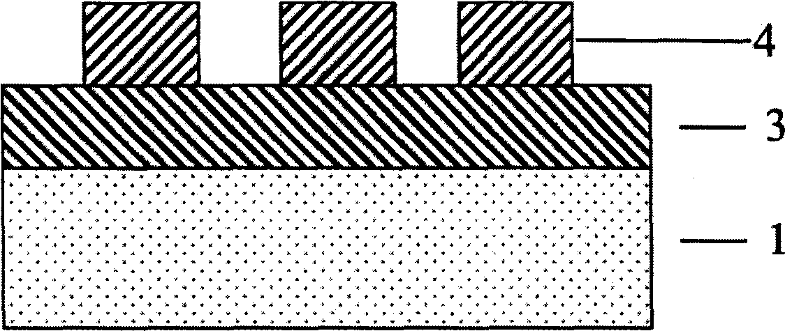
Ions with energy of as 2.0-5.0 Mev are injected into the surface of optic crystal and masks are prepared on the plane optical wave-guides formed. Etching the surface of the optic crystal by using Ar ion beam forms crestiform optical wave-guide. Injecting oxygen ion and silicon ion into non-linear optical crystal such as lithium niobate and barium metaborate forms augment type crestiform optical wave-guide. Infecting helium ion or hydrogen ion into most of optical crystals can form base type crestiform optical wave-guides. The forms crestiform optical wave-guides keep good non-linear properties. Technical parameters can control thickness, width and depth of these crestiform optical wave-guides. The invention can be utilized to produce photoelectronic device for ex. optical switches and optical modulators etc.

Description

(1) Technical field [0001] The invention relates to a method for preparing an optical crystal light waveguide, especially suitable for preparing a ridge-shaped light waveguide of an optical crystal by ion implantation. The invention belongs to a waveguide preparation method in the field of optoelectronic devices. (2) Background technology [0002] Integrated optoelectronics is a signal processing system based on optical waveguide. In this system, the carrier of signal transmission is optical waveguide. Therefore, people use a variety of technologies to develop optical waveguide. Optical waveguide is the basis for manufacturing optoelectronic devices. Optical crystal materials, especially nonlinear optical crystal materials, are of great value for the transmission, conversion, amplification and modulation of optical signals, so the preparation of waveguides on optical crystal materials is very important. The main forming methods of optical waveguide are ion exchange, high te...

Claims


Application Information

Patent Timeline
IPC IPC(8): G02B6/13
Inventor 王雪林陈峰付刚张建华王克明
Owner SHANDONG UNIV
Learn More