Soft-magnetic multilayer film force-sensitive sensor and preparation method thereof
A multi-layer film and sensor technology, applied in the field of sensors, can solve the problems of fragile thin strips, difficult installation, welding, etc., and achieve the effects of easy mass production, low cost, and fast response speed.
- Summary
- Abstract
- Description
- Claims
- Application Information
AI Technical Summary
Problems solved by technology
Method used
Image

Examples
Embodiment 1
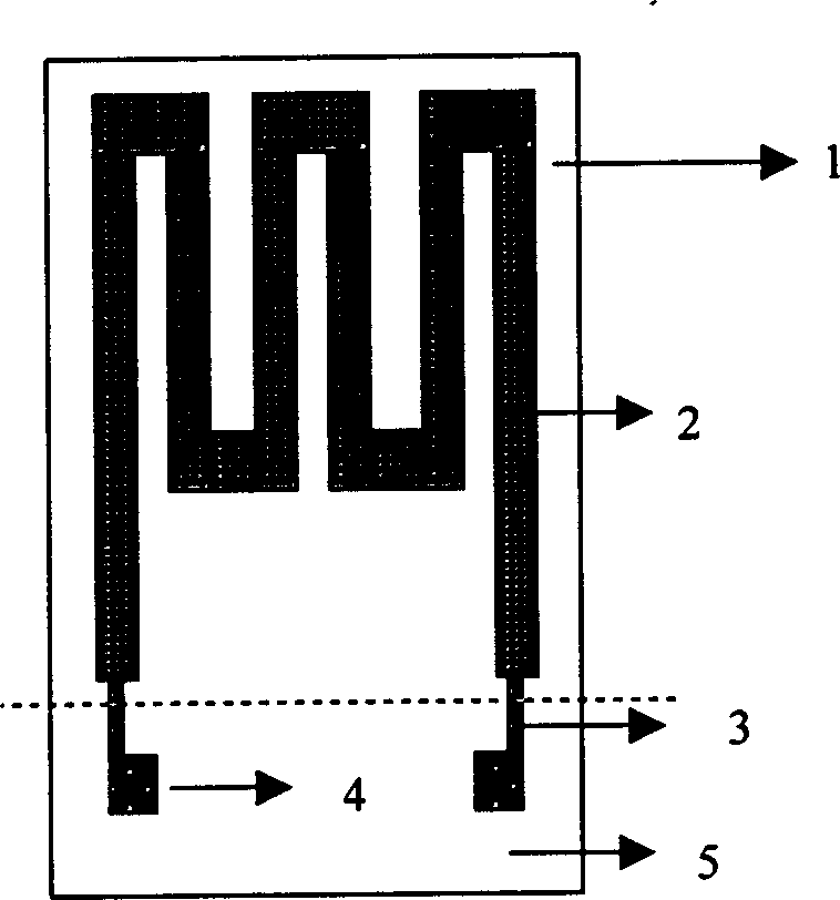
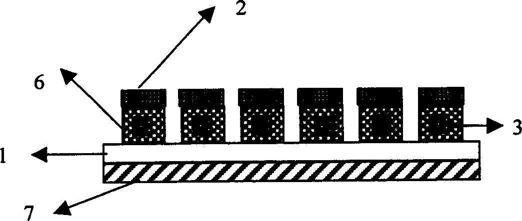
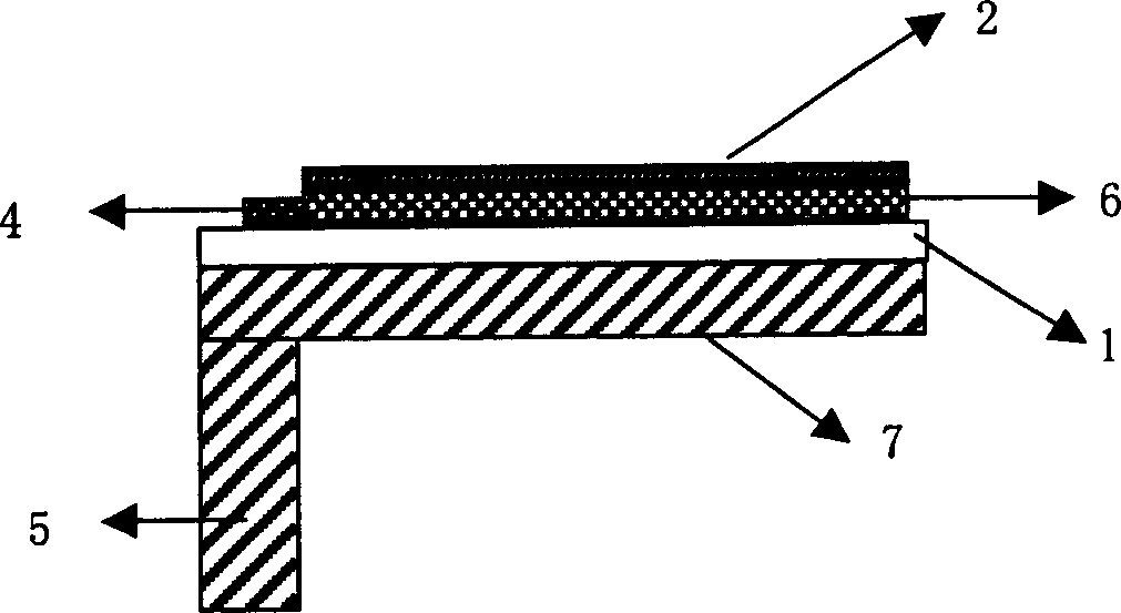
[0059] (1) the double-sided positive glue of the double-sided oxidized silicon substrate 9 that has been cleaned and processed, such as Figure 4 shown. The thickness of the photoresist 8 is 5 μm, the drying temperature of the photoresist is 95 ° C, and the drying time is 1 hour; after double-sided exposure and development, silicon dioxide is etched in BHF etching solution, and finally the photoresist is removed to obtain a double-sided Alignment marks engraved on the surface and windows etched into silicon; Figure 4 Among them, 10 is SiO 2 (2) carry out wet etching to prepare silicon cantilever beam on one side of silicon chip (referred to as A face), as Figure 5 As shown, silicon is etched using potassium hydroxide (KOH) etching solution, the etching temperature is 80°C, and the solution concentration is KOH:H 2 O=44:100, the etching depth is 150 μm; (3) sputtering soft magnetic FeSiB film 11, such as Figure 6 As shown, the thickness of the FeSiB film is 2 μm; (4) spu...
Embodiment 2
[0062] (1) throw positive glue 8 on both sides of the double-sided oxidized silicon wafer substrate that has been cleaned, such as Figure 4 shown. The photoresist thickness is 5 μm, the photoresist drying temperature is 90°C, and the time is 1 hour; after double-sided exposure and development, silicon dioxide is etched in BHF etching solution, and finally the photoresist is removed to obtain a double-sided cover. Engraving alignment symbols and etching silicon windows; (2) performing wet etching on one side of the silicon wafer (called A-side) to prepare silicon cantilever beams, such as Figure 5 As shown, silicon is etched using potassium hydroxide (KOH) etching solution, the etching temperature is 78°C, and the solution concentration is KOH:H 2 O=44:100, etching depth is 150μm; (3) sputtering soft magnetic FeSiB film, such as Figure 6 As shown, the thickness of the FeSiB film is 4 μm; (4) sputtering the underlying Cu, such as Figure 7 As shown, the thickness is 150nm;...
Embodiment 3
[0065] (1) throw positive glue 8 on both sides of the double-sided oxidized silicon wafer substrate that has been cleaned, such as Figure 4 shown. The photoresist thickness is 5 μm, the photoresist drying temperature is 95°C, and the time is 30 minutes; after double-sided exposure and development, silicon dioxide is etched in BHF etching solution, and finally the photoresist is removed to obtain a double-sided overlay Align the symbols and etch the silicon window; (2) perform wet etching on one side of the silicon wafer (referred to as the A side) to prepare the silicon cantilever beam, such as Figure 5 As shown, silicon is etched using potassium hydroxide (KOH) etching solution, the etching temperature is 80°C, and the solution concentration is KOH:H 2 O=44:100, etching depth is 150μm; (3) sputtering soft magnetic FeSiB film, such as Figure 6 As shown, the thickness of the FeSiB film is 6 μm; (4) sputtering the underlying Cu, such as Figure 7 As shown, the thickness is...
PUM
| Property | Measurement | Unit |
|---|---|---|
| width | aaaaa | aaaaa |
| width | aaaaa | aaaaa |
| thickness | aaaaa | aaaaa |
Abstract
Description
Claims
Application Information
 - R&D
- Intellectual Property
- Life Sciences
- Materials
- Tech Scout
- Unparalleled Data Quality
- Higher Quality Content
- 60% Fewer Hallucinations
Browse by: Latest US Patents, China's latest patents, Technical Efficacy Thesaurus, Application Domain, Technology Topic, Popular Technical Reports.
© 2025 PatSnap. All rights reserved.Legal|Privacy policy|Modern Slavery Act Transparency Statement|Sitemap|About US| Contact US: help@patsnap.com