Single electron memory having carbon nano tube structure and process for making it

A carbon nanotube structure and technology of carbon nanotubes, applied in the direction of nanostructure manufacturing, nanotechnology, nanotechnology, etc., can solve problems that plague traditional memory such as power consumption, limited integration, instability of MOS field effect transistors, etc.

Inactive Publication Date: 2006-04-19
INST OF PHYSICS - CHINESE ACAD OF SCI
View PDF0 Cites 0 Cited by
  • Summary
  • Abstract
  • Description
  • Claims
  • Application Information

AI Technical Summary

Problems solved by technology

However, maintaining the trend of continuous scale reduction is facing an extremely serious challenge, that is, the capacitance in the storage unit cannot be too small. If the capacitance is too small to provide enough electrons to the amplifier, the entire memory will be flooded by noise, and the The reliability of information storage cannot be guaranteed; at the same time, the number of electrons in each storage unit will become smaller and smaller with the further improvement of the integration of storage devices, and the MOS field effect transistors in the memory will gradually become unstable.
[0003] In order to continue to maintain the high-speed development of memory devices, people hope to replace traditional memory devices with single-electron memory devices. Metal-oxide-semiconductor field-effect transistor (MOSFET) is used to prepare single-electron dynamic random access memory (J.Appl.Phys.2000, 12, 8594), although this device solves several problems such as power consumption that plague traditional memories, but This device uses the MTJ / MOSFET structure, which limits the further improvement of the integration level, because the size of the MOSFET cannot be too small, otherwise the number of working electrons is too small, which will affect the stability of the device
If the gate of the device is divided into three parts, and the split gate MOSFET is used to reduce the charge required for operation, the integration of the device is lower

Method used


Image

  • Single electron memory having carbon nano tube structure and process for making it
  • Single electron memory having carbon nano tube structure and process for making it
  • Single electron memory having carbon nano tube structure and process for making it

Examples


Embodiment 1

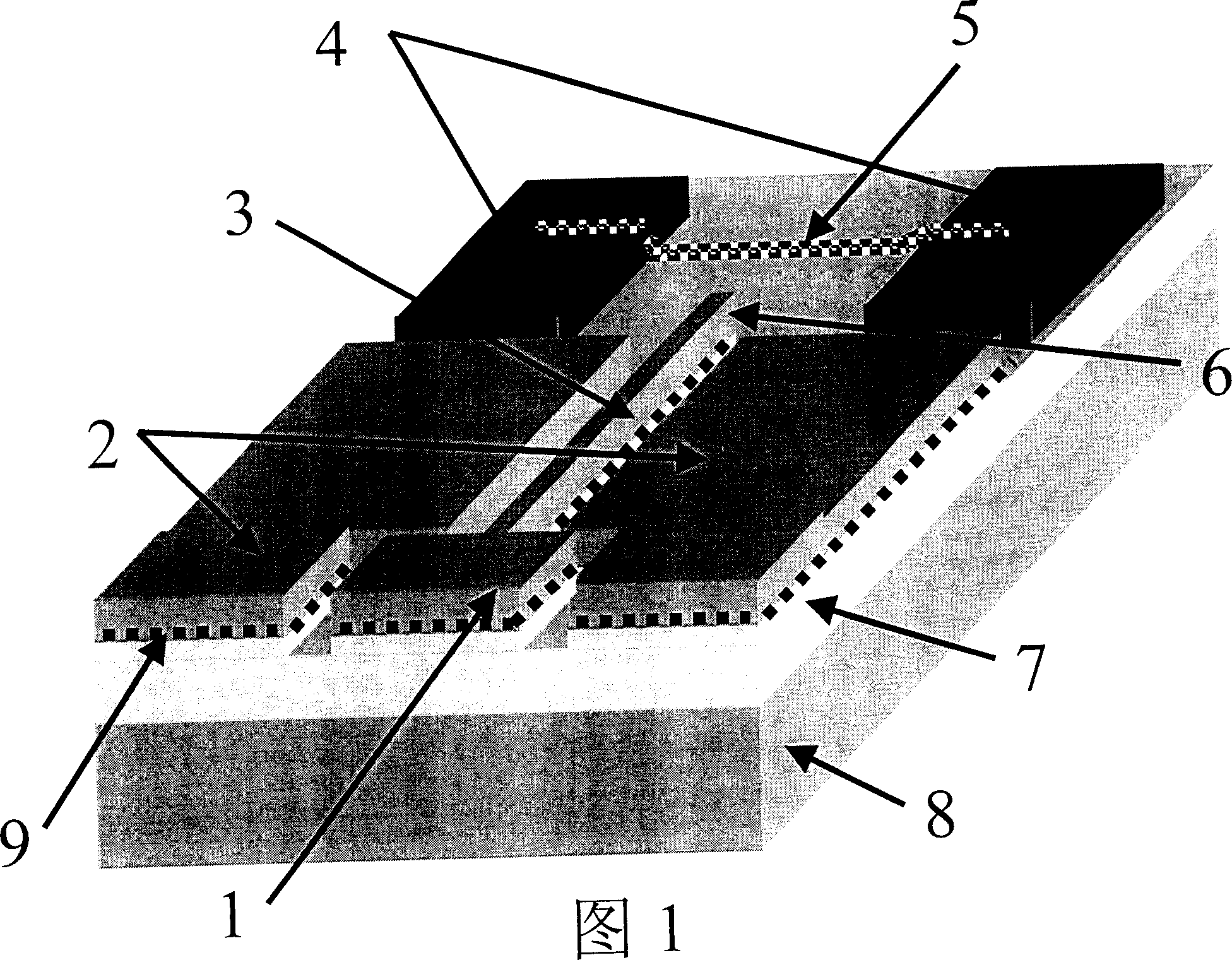
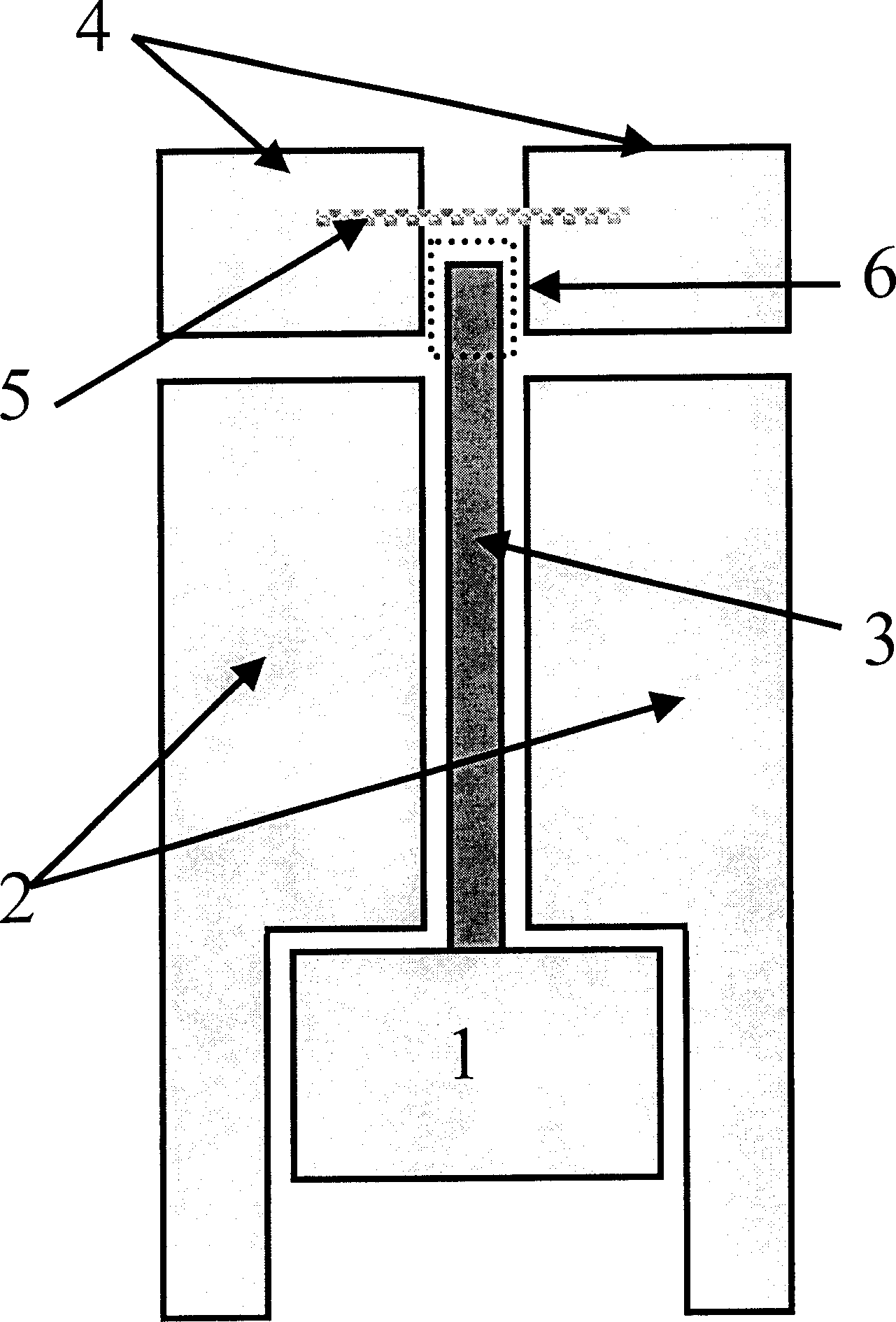
[0047] According to Fig. 1, the single-electron memory with carbon nanotube structure of the present invention is produced.

[0048] Select semi-insulating GaAs as the substrate, and use molecular beam epitaxy (MBE) to grow a GaAs buffer layer with a thickness of 1 micron. The method of molecular beam epitaxy MBE is used to form a GaAs layer 9 containing silicon delta doped on the buffer layer, and this layer is deposited on the GaAs buffer layer with an area density of 1×10 12 cm -2 Silicon and a 50 nm thick GaAs layer grown on it.

[0049] The data line pin 1 , the control gate 2 of the nanowire and the nanowire 3 are prepared by electron beam photolithography and dry etching technology. The depth of the dry etching is 70 nanometers, that is, the δ-doped GaAs layer and part of the buffer layer 7 are etched, as shown in FIG. 1 . The pin width of the data line is 80 nanometers; the size of the control gate of each nanowire is 80 nanometers wide and 80 nanometers long; the l...

Embodiment 2

[0052] According to Fig. 8, the single-electron memory with carbon nanotube structure of the present invention is fabricated.

[0053] The preparation method of the data line pin 1 , the control gate 2 of the nanowire and the nanowire 3 is the same as that of the first embodiment.

[0054] Using photolithography, evaporation and lift-off techniques, gold electrodes were prepared, including two carbon nanotube transistor electrodes 4 with a thickness of 20 nanometers, a width of 50 nanometers, and a length of 100 nanometers, with a distance of 90 nanometers between them. Place catalysts (Fe, Co, Ni and their alloys) on the inner side of the electrode 4 of the carbon nanotube transistor with the probe manipulation technology of the atomic force microscope, and grow the carbon nanotube 5 in situ so that it is in contact with the electrode 4 of the carbon nanotube transistor. If the contact is not good, FIB technology can be used to deposit platinum to form a good ohmic contact be...


PUM


Abstract

The invention relates to a single electron memory having carbon nano tube structure and process for making it. The memory uses the semi-conductive GaAs as substrate, a buffer layer is prepared on the substrate, a Si-containing delta doping GaAs thin layer is prepared on the buffer layer, a nano line is made by etching processing in the delta doping GaAs layer, one end of the nano line is data cable pin, and there are two control grids parallel to the two sides of the namo lines at each side of them. The memory unit is the part of the namo line which is longer the control grid and extending into between the two electrodes of the carbon nano transistor. By controlling several dozens or several electrons, the normal operation of the memory can be realized and without the influence of the random background charges, thus solving the problems such as stability, power consumption, radiation and grid leakage current faced in the development of the traditional memories, the invention also realizes the super-high density information storage under the low power consumption condition.

Description

technical field [0001] The invention relates to a memory device, in particular to a single-electron memory with a carbon nanotube structure and a preparation method. Background technique [0002] Memory accounts for 40% of the world's semiconductor market. Semiconductor products other than memory are updated every 2 years, while memory is a generation every 18 months. Taking the development of dynamic memory (DRAM) as an example, in 1988 Japan The line width of the lines on the silicon chip reached 0.8 microns, and the 4Mb DRAM came out, thus entering the era of ultra-large-scale integration ULSI; in 1992, the 16Mb chip with a line width of 0.5 microns was put into production; in 1994, the 64Mb chip with a line width of 0.35 microns was launched. Chip production; 0.13-micron 4Gb DRAM will soon be realized. However, maintaining the trend of continuous scale reduction is facing an extremely serious challenge, that is, the capacitance in the storage unit cannot be too small. I...

Claims


Application Information

Patent Timeline
Patent Type & Authority Patents(China)
IPC IPC(8): H01L27/00H01L21/70B82B1/00B82B3/00
CPCB82Y10/00B82Y30/00
Inventor 孙劲鹏王太宏
Owner INST OF PHYSICS - CHINESE ACAD OF SCI
Why Eureka
Try Eureka