High-temperature-resistant transparent conductive shielding structure and preparation method thereof
A technology of transparent conduction and shielding structure, applied in the fields of magnetic/electric field shielding, cable/conductor manufacturing, circuit, etc., can solve problems such as smoke, accidents, falling off, etc., to strengthen the force, avoid negative effects, and improve attachment Focus on the effect
- Summary
- Abstract
- Description
- Claims
- Application Information
AI Technical Summary
Problems solved by technology
Method used
Image
Examples
preparation example Construction
[0057] For this reason, the invention provides a kind of preparation method of high temperature resistant transparent conductive shielding structure, comprising:
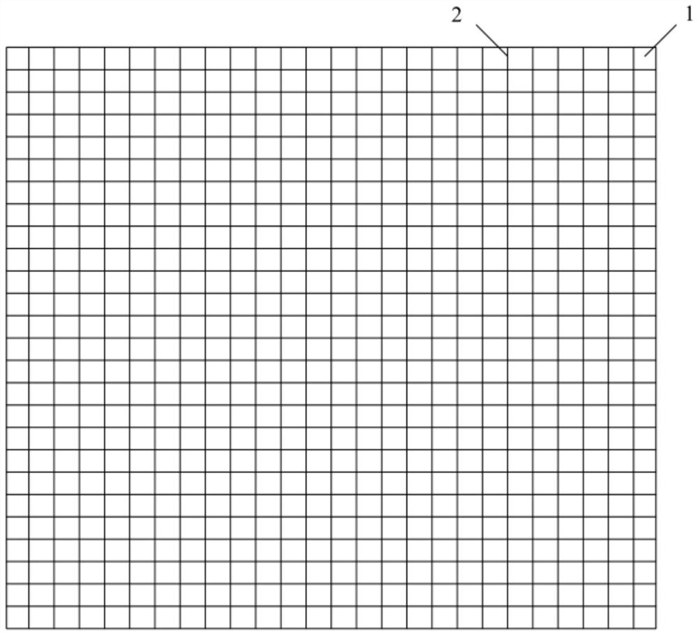
[0058] S101, such as figure 1 As shown, the glass 1 is prepared, and a plurality of thin grooves 11 are formed on the glass, and the plurality of thin grooves 11 are connected to each other to form a hollow network structure;
[0059] Preferably, the width of the fine grooves 11 is 1-100 microns, and the depth is 0.5-20 microns; the maximum distance between adjacent fine grooves 11 is in the range of 100-1000 microns. More preferably, the width of the fine grooves 11 is 10-50 microns, and the depth is 5-15 microns; the maximum distance between adjacent fine grooves 11 is in the range of 260-460 microns.
[0060] The width of the narrow groove 11 is 1-100 microns, which is used to take into account the contradiction between human perception and manufacturing cost. When the width is 1-100 microns, a good naked eye v...
Embodiment 1
[0112] (1) Prepare the glass, form a plurality of thin grooves on the glass by pulsed laser, and connect the plurality of thin grooves to form a hollow network structure. The width of the thin grooves is 40 microns and the depth is 1 micron; adjacent The maximum distance between slots ranges between 260 microns;
[0113] (2) Fill the conductive ink into the fine groove through a soft scraper, the number of times of filling is 5 times, and heat and sinter to form a conductive network;
[0114] (3) On the glass surface that is provided with conductive network body, coating protection liquid, wherein, protection liquid selects polysiloxane for use; Baking is carried out to the glass that coats protection liquid, removes solvent; Ultraviolet light less than 300nm is irradiated to form a transparent protective layer.
Embodiment 2
[0116] (1) Prepare the glass, form a plurality of thin grooves on the glass by pulsed laser, and connect the plurality of thin grooves to form a hollow network structure. The width of the thin grooves is 40 microns and the depth is 5 microns; The maximum distance between slots ranges between 310 microns;
[0117] (2) Fill the conductive ink into the fine groove through a soft scraper, the number of times of filling is 3 times, and heat and sinter to form a conductive network;
[0118] (3) On the glass surface that is provided with conductive network body, coating protection liquid, wherein, protection liquid selects polysiloxane for use; Baking is carried out to the glass that coats protection liquid, removes solvent; Ultraviolet light less than 300nm is irradiated to form a transparent protective layer.
PUM
| Property | Measurement | Unit |
|---|---|---|
| width | aaaaa | aaaaa |
| depth | aaaaa | aaaaa |
| width | aaaaa | aaaaa |
Abstract
Description
Claims
Application Information
 - R&D Engineer
- R&D Manager
- IP Professional
- Industry Leading Data Capabilities
- Powerful AI technology
- Patent DNA Extraction
Browse by: Latest US Patents, China's latest patents, Technical Efficacy Thesaurus, Application Domain, Technology Topic, Popular Technical Reports.
© 2024 PatSnap. All rights reserved.Legal|Privacy policy|Modern Slavery Act Transparency Statement|Sitemap|About US| Contact US: help@patsnap.com


