Preparation method of nanofluidic chip based on carbon nanotubes
A technology of carbon nanotubes and nanotubes, applied in chemical instruments and methods, laboratory containers, laboratory utensils, etc., can solve the problem of precise control, effective control of wall roughness and channel uniformity, and processing resolution depends on Problems such as the nature of the template and the complex manufacturing process, etc., to achieve the effect of rich knowledge and understanding, good uniformity and stability, and precise and controllable dimensions
- Summary
- Abstract
- Description
- Claims
- Application Information
AI Technical Summary
Problems solved by technology
Method used
Image
Examples
Embodiment 1
[0042] Example 1 Basic preparation process of nano flow control chip
[0043] The basic preparation process of the nanofluid chip includes the following steps:
[0044] Step 1, in Si / Sio 2 On-chip etch mark;
[0045] Step 2, in etching good markers Si / Sio 2 Growing carbon nanotube horizontal array on a piece;
[0046] Step three, protect the needed carbon nanotubes by photoresist;
[0047] Step 4, eliminate other excess carbon nanotubes to etiogenize the oxygen plasma;
[0048] Step 5, by photolithography, two separate SU-8 micro-track is constructed on the carbon nanotube;
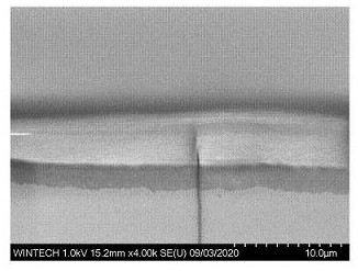
[0049] Step 6. Use FIB precision etching technology to interrupt both ends of the carbon nanotubes;
[0050] Step 7. The pDMS of a pre-punched PDMS is bonded to the surface of the SU-8 microoflow;
[0051] Step 8. Insert the liquid pipe and the liquid pipe in the reserved punch, and the electrode can be inserted into the liquid opening if the electrical measurement is required.
Embodiment 2
[0052]Example 2 The process of protecting the required carbon nanotubes by photoresist
[0053] Huysis: This process uses AZ 1500 4.4CP lithographic positive glue, verification table, in order to obtain a thickness of 1 um, the speed is set to 500 rpm 10s, and then 2000 rpm 30s.
[0054] Front baking: baked for 1 min at 100 ° C above the hot plate.
[0055] Exposure: G-line contact exposure machine exposure 5s.
[0056] Development: Soak the substrate in the sink with AZ300MIF (2.38%) for 1 min.
[0057] Cleaning: Clean 30s with deionized water.
Embodiment 3
[0058] Example 3 The process of constructing micro tracking
[0059] Homorite: Add the SU-8 2050 lithography negatively to the substrate, and the substrate is attached to the hierarchy machine for a period of time. According to the structure of the thickness 50 um, the speed is set to 500 rpm 10s, and then 3000 rpm 30s.
[0060] Front baking: It was baked at 65 ° C for 4 min on the hot plate, and then baked 9 min at 95 ° C. A piece of filter paper is then placed in a large plastic culture dish, and the hot silicon wafer is placed on the filter paper to room temperature.
[0061] Exposure: Contactless exposure machine exposure 20s.
[0062] After the hot plate, it was baked at 65 ° C for 2 min first, then baked at 95 ° C for 7 min. A piece of filter paper is then placed in a large plastic culture dish, and the hot silicon wafer is placed on the filter paper to room temperature.
[0063] Development: It is completely immersed in the developer for 7 minutes, and then the Fresh develo...
PUM
| Property | Measurement | Unit |
|---|---|---|
| diameter | aaaaa | aaaaa |
Abstract
Description
Claims
Application Information
 - Generate Ideas
- Intellectual Property
- Life Sciences
- Materials
- Tech Scout
- Unparalleled Data Quality
- Higher Quality Content
- 60% Fewer Hallucinations
Browse by: Latest US Patents, China's latest patents, Technical Efficacy Thesaurus, Application Domain, Technology Topic, Popular Technical Reports.
© 2025 PatSnap. All rights reserved.Legal|Privacy policy|Modern Slavery Act Transparency Statement|Sitemap|About US| Contact US: help@patsnap.com


