


Quick Research
Generate reliable direction feasibility study reports for your R&D in just a few steps.

Technical Q&A
Discover and master advanced knowledge NOW. Basics, ideas, possibilities, all at once.

Find Solutions
As an expert in R&D theories, this can generate solutions to your technical problems instantly.

Evaluate Feasibility
Analyze your overall solution with one click, know your potential R&D risks in advance.

Monitor Landscape
Get weekly tech updates, stay abreast of the latest tech innovations and key insights.
Low-temperature semiconductor direct bonding method based on surface modification and activation
A direct bonding and surface modification technology, which is applied in the field of solar cells, can solve the problems of commercialization of multi-junction solar cells, and achieve the effects of batch preparation, improved photoelectric conversion efficiency, and good interface crystallization quality
- Summary
- Abstract
- Description
- Claims
- Application Information
AI Technical Summary
Problems solved by technology
Method used
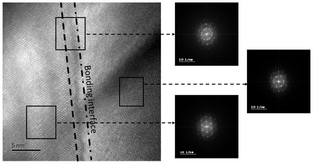
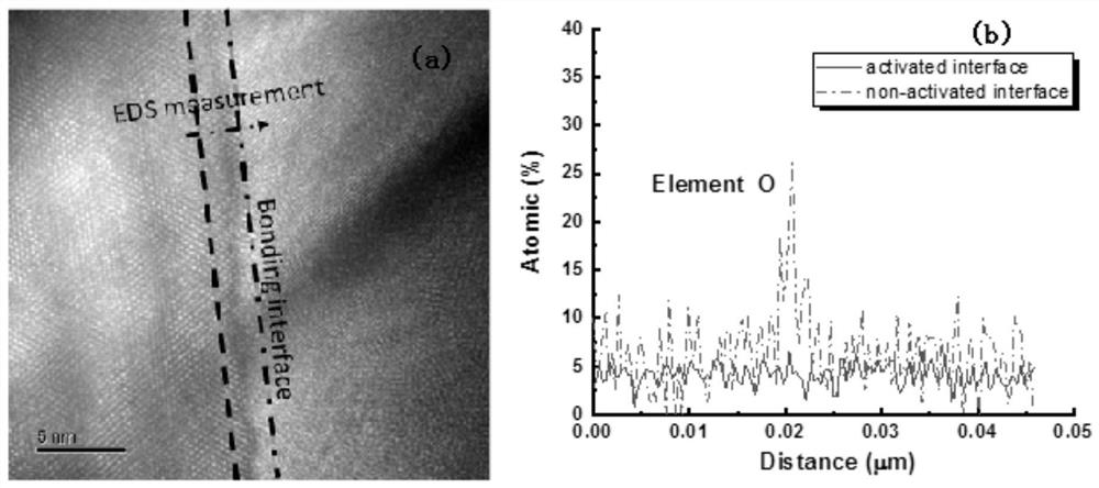
Image

Examples
Embodiment 1
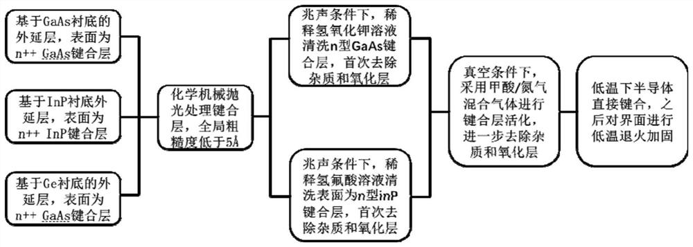
[0027] This embodiment discloses a method for preparing a 5-junction solar cell based on direct bonding of surface modification and activated low-temperature semiconductor, including the following steps:
[0028] 1. Sub-battery epitaxial growth and structure:
[0029] (1) The thickness is 350 μm, the crystal orientation is (100), and the doping concentration is about 10 17 cm -3 ~10 18 cm -3 The n-type GaAs wafer is used as the substrate, and the three-junction sub-cell structure is epitaxially grown on the GaAs substrate by metal-organic vapor phase epitaxy (MOVPE), which in turn includes (Al x Ga 1-x ) y In 1-y P subcell structure, fourth tunnel junction structure, Al with a bandgap of 1.7eV x Ga 1-x As sub-cell structure, the third tunnel junction structure, GaAs sub-cell structure with a band gap of 1.4eV and the second tunnel junction structure; the specific content (x, y values) of Al, Ga, In and other components can be determined by the material The band gap is...
Embodiment 2
[0041] This embodiment discloses a method for preparing a 4-junction solar cell based on direct bonding of surface modification and activated low-temperature semiconductor, including the following steps:
[0042] 1. Sub-battery epitaxial growth and structure:
[0043] (1) The thickness is 350 μm, the crystal orientation is (100), and the doping concentration is about 10 17 -10 18 cm -3 The n-type GaAs wafer is used as the substrate, and the metal-organic vapor phase epitaxy (MOVPE) is used to epitaxy the two-junction sub-cell structure on the substrate, followed by GaxIn with a bandgap width of 1.8eV 1-x The P subcell structure, the third tunnel junction structure, the GaAs subcell structure with a bandgap of 1.4eV, and the second tunnel junction structure; the specific content (x value) of Ga, In and other components can be determined by the material band The gap is calculated; the tunnel junction is mainly composed of a thickness of only a dozen nanometers and a doping co...
PUM
| Property | Measurement | Unit |
|---|---|---|
| thickness | aaaaa | aaaaa |
| thickness | aaaaa | aaaaa |
| thickness | aaaaa | aaaaa |
Abstract
Description
Claims
Application Information
 - R&D Engineer
- R&D Manager
- IP Professional
- Industry Leading Data Capabilities
- Powerful AI technology
- Patent DNA Extraction
Browse by: Latest US Patents, China's latest patents, Technical Efficacy Thesaurus, Application Domain, Technology Topic, Popular Technical Reports.
© 2024 PatSnap. All rights reserved.Legal|Privacy policy|Modern Slavery Act Transparency Statement|Sitemap|About US| Contact US: help@patsnap.com