
Growth method for spin-coating single crystal on wide bandgap semiconductor substrate

A wide-bandgap semiconductor and growth method technology, which is applied to the growth field of spin-coated single crystals on wide-bandgap semiconductor substrates, can solve the problems of complex processes, harsh growth conditions, and expensive equipment, and achieves high crystal quality and defects. Density reduction effect

Pending Publication Date: 2020-06-05
GUANGXI UNIV
View PDF5 Cites 3 Cited by
  • Summary
  • Abstract
  • Description
  • Claims
  • Application Information

AI Technical Summary

Problems solved by technology

[0006] (1) The existing method of using the solubility difference of perovskite in a certain solvent at different temperatures to precipitate perovskite single crystal particles can only grow three-dimensional single crystals, not two-dimensional single crystal films, which is not conducive to large-scale application
[0007] (2) The existing methods for growing lead iodide single crystals are complex and expensive, which hinders the application of lead iodide optoelectronic devices
At present, the growth methods of lead iodide single crystals include Bridgman method and evaporation method, which require high temperature and high vacuum, harsh growth conditions, and slow growth rate, which are not suitable for large-scale production of lead iodide single crystals.

Method used


Image

  • Growth method for spin-coating single crystal on wide bandgap semiconductor substrate
  • Growth method for spin-coating single crystal on wide bandgap semiconductor substrate
  • Growth method for spin-coating single crystal on wide bandgap semiconductor substrate

Examples


Embodiment 1

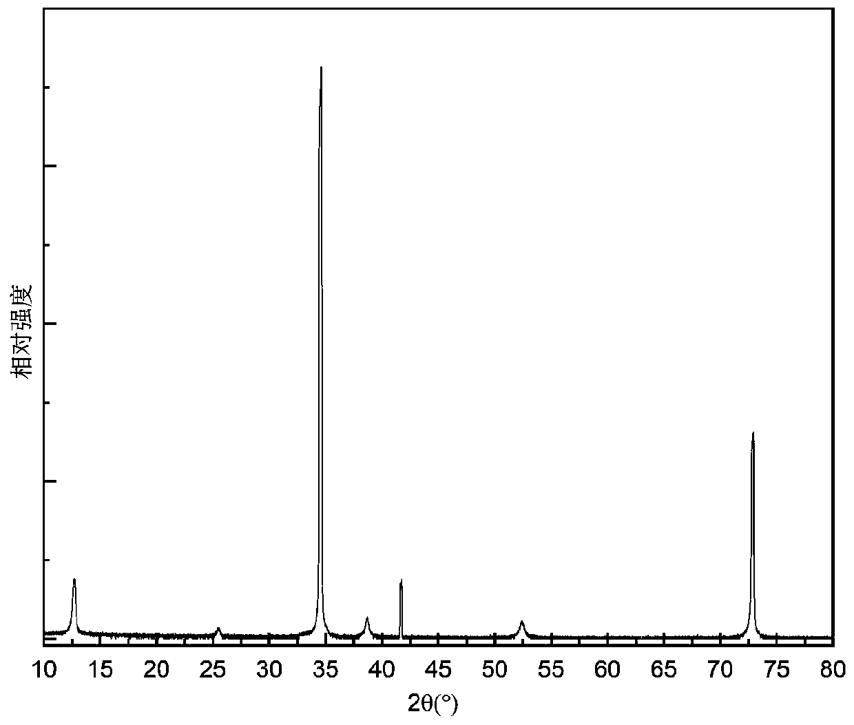
[0057] see image 3 The XRD diffraction pattern of the lead iodide film, the lead iodide material was grown on the thoroughly cleaned gallium nitride substrate by the spin coating process, and a high-quality single-oriented epitaxial lead iodide single crystal film was obtained, and the lead iodide was only Clusters of {001} facets appear. Wherein, the substrate may be any one or a composite substrate formed of aluminum gallium nitride, indium gallium nitride, gallium nitride, aluminum nitride or silicon carbide substrates. The solute of the lead iodide precursor solution is lead iodide powder with a purity greater than 99.9%, and the solvent is a mixed solution of N,N-dimethylformamide and dimethyl sulfoxide, wherein N,N-dimethylformamide The ratio to dimethyl sulfoxide is about 4:1. The concentration of the lead iodide precursor solution is 0.5 moles per liter to 2 moles per liter. The lead iodide precursor solution was stirred at about 70° C. for 2 hours on a heated stir...

Embodiment 2

[0059] see Figure 4 XRD diffraction pattern of perovskite, high-quality epitaxial perovskite CsPbBrI was obtained by growing perovskite material on single crystal silicon substrate by spin-coating process 2 For single crystal thin films, only (200) crystal planes appear in perovskite. Wherein, the substrate may be any one or a composite substrate formed of aluminum gallium nitride, indium gallium nitride, gallium nitride, aluminum nitride or silicon carbide substrates. The solute of the precursor solution of the perovskite solution is lead iodide powder, lead bromide powder, cesium iodide powder and cesium bromide powder, and the solvent is N,N-dimethylformamide and dimethyl sulfoxide A mixed solution, wherein the ratio of N,N-dimethylformamide to dimethyl sulfoxide is 1:1. The concentration of the perovskite solution is 0.3 to 0.5 moles per liter. The perovskite solution precursor solution was stirred at about 70 °C for 2 hours on a heated stirring table to obtain a clear...


PUM


Abstract

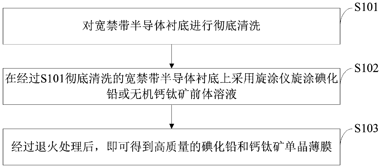
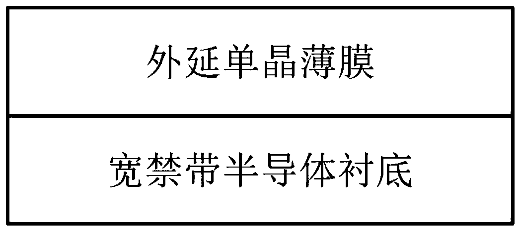
The invention belongs to the technical field of perovskite solar cells, photoelectric detectors and wide bandgap semiconductor photoelectric materials and devices, and discloses a growth method for spin-coating single crystal on a wide bandgap semiconductor substrate. The growth method comprises the following steps: respectively cleaning the wide bandgap semiconductor substrate for 30 minutes by using isopropanol, ethanol and deionized water in an ultrasonic cleaning machine, treating the substrate for 15 minutes by using ultraviolet ozone, and thoroughly cleaning the wide bandgap semiconductor substrate; spin-coating lead iodide or an inorganic perovskite precursor solution on the thoroughly cleaned wide bandgap semiconductor substrate by using a spin coater; and carrying out annealing treatment to obtain the high-quality lead iodide and perovskite single crystal film. The invention discloses a technology for growing a high-quality lead iodide and perovskite single crystal thin film by adopting a spin-coating process. By optimizing the proportion of a precursor solution and the growth temperature of the film, lead iodide or a perovskite material grows on the wide bandgap semiconductor substrate by using the spin-coating process, and a high-quality epitaxial single crystal film is obtained and is applied to manufacturing of an efficient photoelectric detector or a solar cell.

Description

technical field [0001] The invention belongs to the technical field of perovskite solar cells, photodetectors, and wide-bandgap semiconductor optoelectronic materials and devices, and relates to a method for growing a spin-coated single crystal on a wide-bandgap semiconductor substrate, in particular to a method for growing a wide-bandgap semiconductor A method for growing high-quality lead iodide and perovskite single crystal thin films on substrates by spin-coating process. Background technique [0002] In recent years, perovskite has attracted great attention from researchers due to its advantages such as high light absorption coefficient, low exciton binding energy and long carrier diffusion distance. In just ten years, perovskite solar cells The photoelectric conversion efficiency has been increased from 3.8% to over 23%. Since the preparation process is very similar to traditional organic / polymer optoelectronic devices, perovskite optoelectronic devices are widely use...

Claims


Application Information

Patent Timeline
Patent Type & Authority Applications(China)
IPC IPC(8): C30B29/12C30B19/00
CPCC30B19/00C30B29/12
Inventor 孙文红王玉坤李磊
Owner GUANGXI UNIV
Learn More