A spintronic device and preparation method for realizing visible light-controlled interfacial magnetism
A spintronic device, visible light technology, applied in field-controlled resistors, parts of electromagnetic equipment, manufacturing/processing of electromagnetic devices, etc. question
- Summary
- Abstract
- Description
- Claims
- Application Information
AI Technical Summary
Problems solved by technology
Method used
Image
Examples
preparation example Construction
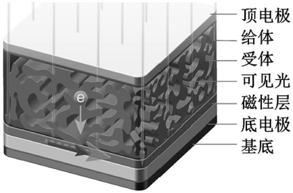
[0037] A method for preparing a spintronic device capable of controlling interfacial magnetism by visible light, comprising the following steps:
[0038] 1) setting the bottom electrode on the substrate;
[0039] 2) setting a magnetic layer on the bottom electrode;
[0040] 3) disposing the active layer solution on the magnetic layer;
[0041] 4) A layer of top electrode is arranged on the active layer.
[0042] The thickness of the bottom electrode is 3nm-8nm, the thickness of the magnetic layer is 0.5nm-20nm, the atmosphere is air, the thickness of the film is controlled by a quartz crystal microbalance during the preparation process, and no in-situ annealing treatment is performed after the preparation.
[0043] The organic active layer is a polymer solution in which the ratio of donor to acceptor is 1:1 to 1:5 and the concentration is 5 to 20 mg·mL -1 , the solvent is a mixed solution of 1,8-diiodooctane and o-xylene, wherein the volume fraction of 1,8-diiodooctane is 1...
Embodiment 1
[0048] A method for preparing a spintronic device capable of controlling interfacial magnetism by visible light, comprising the following steps:
[0049] Step 1: Using Si / SiO 2 As the substrate, a Ta film was deposited on the substrate by DC magnetron sputtering at room temperature, and Ta was used as the bottom electrode.
[0050] The specific process is: the thickness is 5nm.
[0051] Step 2: using a DC magnetron sputtering method to deposit a Co thin film on Ta at room temperature, and the Co thin film is used as a magnetic layer.
[0052] The specific process is: the thickness is 0.9nm.
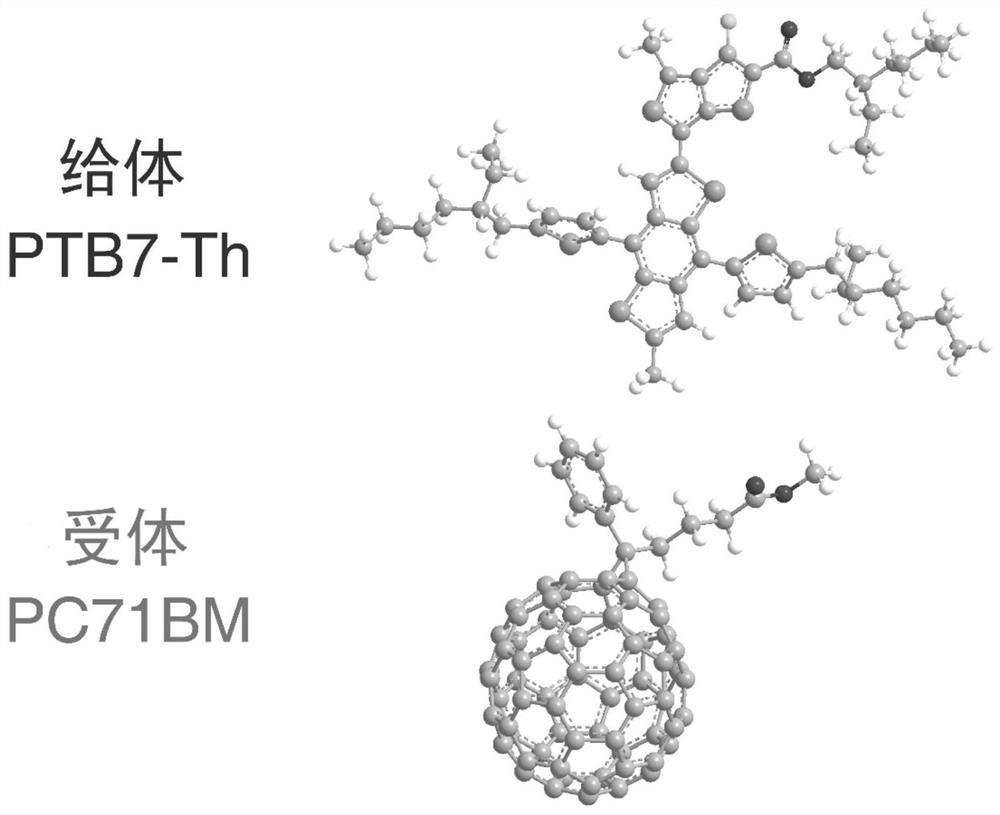
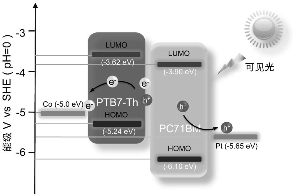
[0053] Step 3: Using PTB7-Th and PC71BM polymer solutions, the organic active layer was spin-coated onto Si / SiO using a DC magnetron sputtering method at room temperature 2 / Ta / Co on.
[0054] The specific polymer solution process is: 1) The solvent is a mixed solution of 1,8-diiodooctane and o-xylene, wherein the volume fraction of 1,8-diiodooctane is 3%; 2) The donor and acceptor T...
Embodiment 2
[0059] The difference between this embodiment and Embodiment 1 is that the thickness of Co is 1 nm, and the rest are the same as Embodiment 1.
[0060] The basic principle of this embodiment is the same as that of Embodiment 1, changing the thickness of the Co layer will change its shape anisotropy and charge density, thereby changing the control of the interfacial magnetism.
[0061] For the SiO prepared by the above-mentioned embodiment 2 / Si / Ta / Co / PTB7-Th: PC71BM / Pt photovoltaic spintronic devices are tested, the simulated light source is 1.5 times the solar power density, and the test results are as follows Figure 4 shown.
PUM
| Property | Measurement | Unit |
|---|---|---|
| thickness | aaaaa | aaaaa |
| thickness | aaaaa | aaaaa |
| thickness | aaaaa | aaaaa |
Abstract
Description
Claims
Application Information
 - R&D
- Intellectual Property
- Life Sciences
- Materials
- Tech Scout
- Unparalleled Data Quality
- Higher Quality Content
- 60% Fewer Hallucinations
Browse by: Latest US Patents, China's latest patents, Technical Efficacy Thesaurus, Application Domain, Technology Topic, Popular Technical Reports.
© 2025 PatSnap. All rights reserved.Legal|Privacy policy|Modern Slavery Act Transparency Statement|Sitemap|About US| Contact US: help@patsnap.com


