


Quick Research
Generate reliable direction feasibility study reports for your R&D in just a few steps.

Technical Q&A
Discover and master advanced knowledge NOW. Basics, ideas, possibilities, all at once.

Find Solutions
As an expert in R&D theories, this can generate solutions to your technical problems instantly.

Evaluate Feasibility
Analyze your overall solution with one click, know your potential R&D risks in advance.

Monitor Landscape
Get weekly tech updates, stay abreast of the latest tech innovations and key insights.
Easy-resist removing high-energy ion implantation multilayer mask manufacturing method
A multi-layer mask, high-energy ion technology, used in semiconductor/solid-state device manufacturing, electrical components, circuits, etc., can solve the problems of complex and difficult processes, multiple lithography and etching, etc.
- Summary
- Abstract
- Description
- Claims
- Application Information
AI Technical Summary
Problems solved by technology
Method used
Image


Examples
Embodiment 1
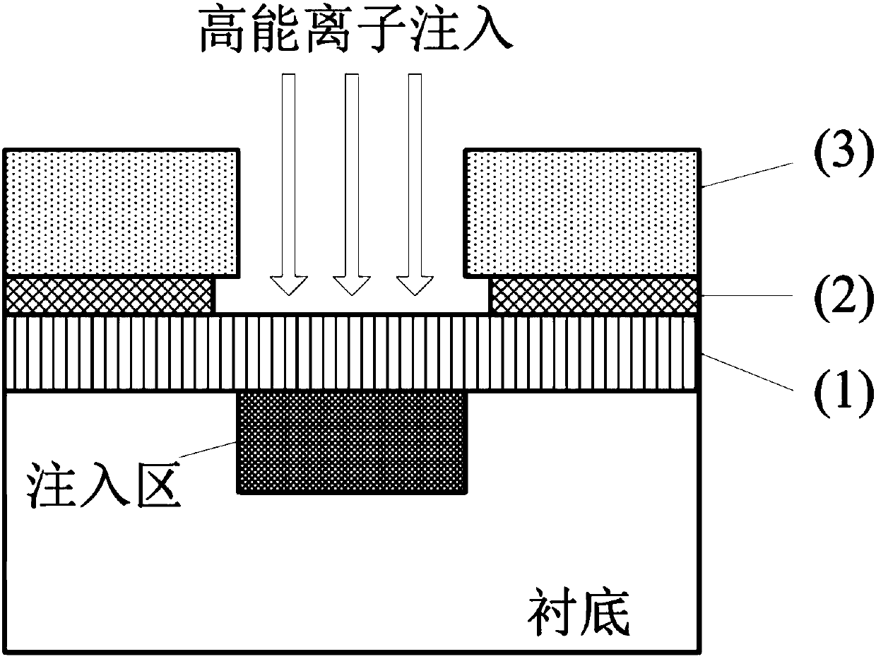
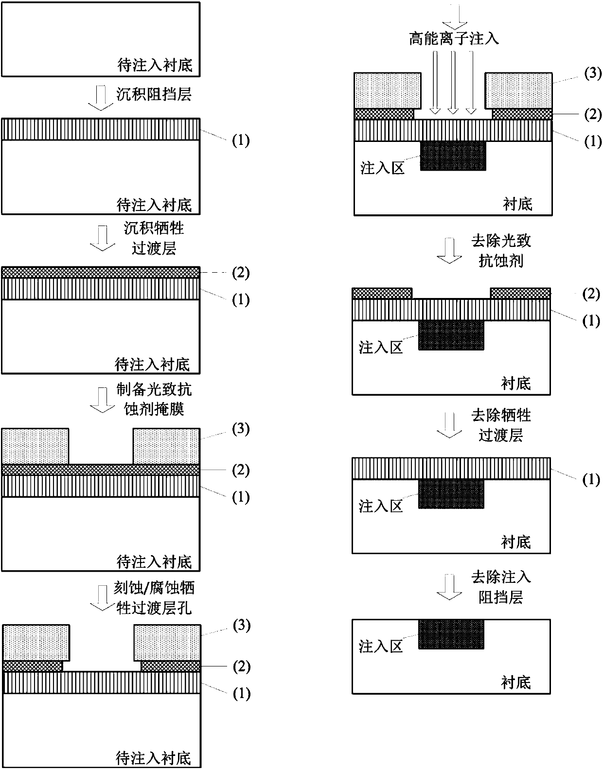
[0026] A 40nm thick cadmium telluride thin film is thermally evaporated and deposited on the substrate as an injection barrier layer, and then a 70nm thick zinc sulfide thin film is thermally evaporated and deposited as a sacrificial transition layer, according to the thickness of the sacrificial transition layer zinc sulfide≤implantation area Outer expansion error limit / tan (ion incident angle), for an implantation region outreach error of 0.1 μm and an implantation inclination angle of 7°, the condition is satisfied if the thickness of the zinc sulfide layer is less than 800 nm.
[0027] Clean and dry the chip on which the injection barrier layer and sacrificial transition layer have been deposited, spin-coat photoresist AZ1500 on the surface of the chip, and selectively expose and develop the chip to define the photoresist mask injection Area.
[0028] Using the photoresist injection area pattern as an etching mask, use pure hydrochloric acid at 0°C to corrode the injection...
Embodiment 2
[0031] A 300nm thick cadmium telluride thin film is thermally evaporated and deposited on the substrate as an injection barrier layer, and then a 300nm thick zinc sulfide thin film is thermally evaporated deposited as a sacrificial transition layer, according to the thickness of the sacrificial transition layer zinc sulfide ≤ implantation area Outer expansion error limit / tan (ion incident angle), for an implantation region outreach error of 0.1 μm and an implantation inclination angle of 7°, the condition is satisfied if the thickness of the zinc sulfide layer is less than 800 nm.
[0032] Clean and dry the chip on which the injection barrier layer and sacrificial transition layer have been deposited, spin-coat photoresist AZ5200 on the surface of the chip, and selectively expose and develop the chip to define the photoresist mask injection Area.
[0033]Using the photoresist implanted area pattern as an etching mask, use pure hydrochloric acid at 0°C to corrode the implanted ...
Embodiment 3
[0036] A 200nm-thick cadmium telluride thin film is thermally evaporated and deposited on the substrate as an injection barrier layer, and then a 70nm-thick zinc sulfide thin film is thermally evaporated deposited as a sacrificial transition layer, according to the thickness of the sacrificial transition layer zinc sulfide≤implantation area Outer expansion error limit / tan (ion incident angle), for an implantation region outreach error of 0.1 μm and an implantation inclination angle of 7°, the condition is satisfied if the thickness of the zinc sulfide layer is less than 800 nm.
[0037] Clean and dry the chip on which the injection barrier layer and sacrificial transition layer have been deposited, spin-coat photoresist AZ5200 on the surface of the chip, and selectively expose and develop the chip to define the photoresist mask injection Area.
[0038] Using the photoresist implanted region pattern as an etching mask, Ar:CH 4 :H 2 The mixed gas is an etching gas, and the zin...
PUM
 Abstract
Description
Claims
Application Information
 - R&D Engineer
- R&D Manager
- IP Professional
- Industry Leading Data Capabilities
- Powerful AI technology
- Patent DNA Extraction
Browse by: Latest US Patents, China's latest patents, Technical Efficacy Thesaurus, Application Domain, Technology Topic, Popular Technical Reports.
© 2024 PatSnap. All rights reserved.Legal|Privacy policy|Modern Slavery Act Transparency Statement|Sitemap|About US| Contact US: help@patsnap.com