Adhesive tape for protecting semiconductor wafer surface and method for processing semiconductor wafer
A processing method and semiconductor technology, which can be used in semiconductor/solid-state device manufacturing, film/sheet-like adhesives, adhesives, etc., and can solve the problems of increased adhesion of surface protection tapes, poor peeling of wafers, and reduced peelability. Achieve the effect of excellent adhesion, excellent peelability, and less edge bulge
- Summary
- Abstract
- Description
- Claims
- Application Information
AI Technical Summary
Problems solved by technology
Method used
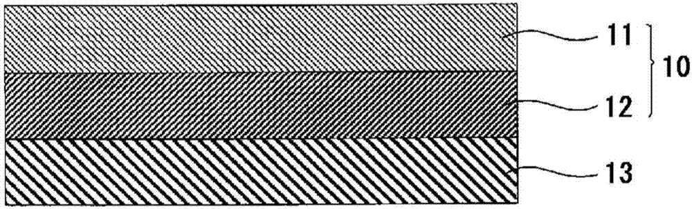
Image

Examples
Embodiment 1
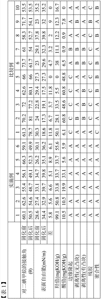
[0198] 50 parts by mass of a urethane acrylate oligomer (manufactured by Shin-Nakamura Chemical Industry Co., Ltd.) with a weight average molecular weight of 3500, 50 parts by mass of isobornyl acrylate, and Irgacure 184 (manufactured by BASF) as a photopolymerization initiator were mixed. ) 5.0 parts by mass to obtain an ultraviolet curable resin composition. The obtained ultraviolet curable resin composition was coated on a PET film (manufactured by Toray Co., Ltd.: thickness 38 μm) as a casting process sheet with a thickness of 270 μm by a fountain die method to form a resin combination. object layer. Immediately after coating, the same PET film was further laminated on the resin composition layer, and thereafter, a high-pressure mercury lamp (160 W / cm, height 10 cm) was used to emit light at 500 mJ / cm 2 Under the condition of ultraviolet ray irradiation, the resin composition layer was crosslinked / cured, and a base film with a thickness of 270 μm was obtained.
[0199] 1...
Embodiment 2
[0203] 2.0 mol% of methacrylic acid, 70 mol% of 2-ethylhexyl acrylate, and 28 mol% of 2-hydroxyethyl acrylate were mixed and polymerized in a solution to obtain a polymer solution. In the solution, 10 parts by mass of 2-methacryloyloxyethyl isocyanate (manufactured by Showa Denko Co., Ltd., Karenz MOI) was mixed with 100 parts by mass of the polymer to introduce an ethylenically unsaturated group into the hydroxyl group , thereby synthesizing an ethylenically unsaturated group-containing acrylic copolymer polymer (weight average molecular weight: 500,000, hydroxyl value: 50.8 mgKOH / g, acid value: 10.5 mgKOH / g).
[0204] In this ethylenically unsaturated group-containing acrylic copolymer polymer, 0.5 parts by mass of CORONET L (manufactured by Nippon Polyurethane Industry Co., Ltd.) as a crosslinking agent and Irgacure 184 (manufactured by BASF Corporation) as a photopolymerization initiator were mixed. ) 5.0 parts by mass to obtain an adhesive composition.
[0205] The obtai...
Embodiment 3
[0207] 4.0 mol% of methacrylic acid, 76 mol% of 2-ethylhexyl acrylate, and 20 mol% of 2-hydroxyethyl acrylate were mixed and polymerized in a solution to obtain a polymer solution. In the solution, 10 parts by mass of 2-acryloyloxyethyl isocyanate (manufactured by Showa Denko Co., Ltd., Karenz AOI) was mixed with 100 parts by mass of the polymer to introduce an ethylenically unsaturated group into the hydroxyl group. This synthesized an ethylenically unsaturated group-containing acrylic copolymer polymer (weight average molecular weight: 350,000, hydroxyl value: 33.8 mgKOH / g, acid value: 19.9 mgKOH / g).
[0208] 1.5 parts by mass of CORONET L (manufactured by Nippon Polyurethane Industry Co., Ltd.) and 0.3 parts by mass of TETRAD-X (manufactured by Mitsubishi Gas Chemical Co., Ltd.) were mixed with this ethylenically unsaturated group-containing acrylic copolymer polymer. Parts by mass, 5.0 parts by mass of Irgacure 651 (manufactured by BASF) as a photopolymerization initiator,...
PUM
| Property | Measurement | Unit |
|---|---|---|
| acid value | aaaaa | aaaaa |
| acid value | aaaaa | aaaaa |
| height | aaaaa | aaaaa |
Abstract
Description
Claims
Application Information
 - Generate Ideas
- Intellectual Property
- Life Sciences
- Materials
- Tech Scout
- Unparalleled Data Quality
- Higher Quality Content
- 60% Fewer Hallucinations
Browse by: Latest US Patents, China's latest patents, Technical Efficacy Thesaurus, Application Domain, Technology Topic, Popular Technical Reports.
© 2025 PatSnap. All rights reserved.Legal|Privacy policy|Modern Slavery Act Transparency Statement|Sitemap|About US| Contact US: help@patsnap.com