


Quick Research
Generate reliable direction feasibility study reports for your R&D in just a few steps.

Technical Q&A
Discover and master advanced knowledge NOW. Basics, ideas, possibilities, all at once.

Find Solutions
As an expert in R&D theories, this can generate solutions to your technical problems instantly.

Evaluate Feasibility
Analyze your overall solution with one click, know your potential R&D risks in advance.

Monitor Landscape
Get weekly tech updates, stay abreast of the latest tech innovations and key insights.
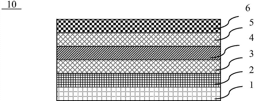
Method for preparing silicon thin film light and heat absorber
A technology of absorber and silicon thin film, which is applied in the field of preparation of multilayer thin film materials, can solve the problems of low service life and poor wear resistance, and achieve the effects of good heat resistance, uniform refractive index and high hardness
- Summary
- Abstract
- Description
- Claims
- Application Information
AI Technical Summary
Problems solved by technology
Method used
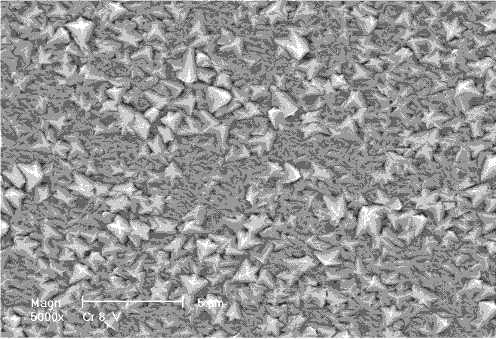
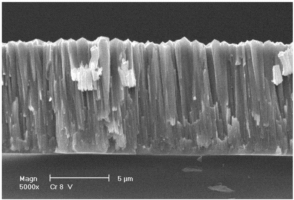
Image

Examples
Embodiment 1
[0032] A method for preparing a silicon thin film photothermal absorber, comprising the following steps:
[0033] Step 1 Clean the stainless steel substrate 1, dry it with high-pressure nitrogen, place it in the vacuum coating chamber, and evacuate it to 10 -4 Pa, fill in the working gas argon, the gas flow rate is 200SCCM, adjust the gate valve to the working pressure of 1Pa, turn on the intermediate frequency pulse power supply, stimulate the plasma to clean the surface of the workpiece for 10 minutes, turn on the chromium oxide target baffle and the electron emission source , after 20 minutes of deposition by PEMS method, the chromium trioxide target baffle and the electron emission source are closed to form the first chromium trioxide thin film layer 2 with a thickness of 200nm 。
[0034] Step 2 Open the silver target baffle and the electron emission source, and close the silver target baffle and the electron emission source after 5 minutes of deposition to form a silver ...
Embodiment 2
[0040] Step 1 Clean the stainless steel substrate, dry it with high-pressure nitrogen, place it in the vacuum coating chamber, and evacuate it to 10 -4 Pa, fill in the working gas argon, the gas flow rate is 250SCCM, adjust the gate valve to the working pressure of 1.5Pa, turn on the intermediate frequency pulse power supply, stimulate the plasma to clean the workpiece surface for 10 minutes, turn on the chromium oxide target baffle and electron emission Source, after 15 minutes of deposition by PEMS method, close the chromium trioxide target baffle and the electron emission source to form the first chromium trioxide thin film layer with a thickness of 180nm.
[0041] Step 2: Turn on the silver target baffle and the electron emission source, and close the silver target baffle and the electron emission source after 3 minutes of deposition to form a silver thin film layer with a thickness of 170nm.
[0042] Step 3: Open the chromium trioxide target baffle and the electron emissi...
PUM
| Property | Measurement | Unit |
|---|---|---|
| Grain size | aaaaa | aaaaa |
| Thickness | aaaaa | aaaaa |
| Thickness | aaaaa | aaaaa |
Abstract
Description
Claims
Application Information
 - R&D Engineer
- R&D Manager
- IP Professional
- Industry Leading Data Capabilities
- Powerful AI technology
- Patent DNA Extraction
Browse by: Latest US Patents, China's latest patents, Technical Efficacy Thesaurus, Application Domain, Technology Topic, Popular Technical Reports.
© 2024 PatSnap. All rights reserved.Legal|Privacy policy|Modern Slavery Act Transparency Statement|Sitemap|About US| Contact US: help@patsnap.com