
Redundant doping radiation-proof MOS (Metal Oxide Semiconductor) field-effect tube based on 65nm process

A field-effect transistor, anti-radiation technology, applied in electrical components, circuits, semiconductor devices, etc., can solve the problems of sub-threshold swing degradation, device failure, device threshold voltage drift, etc., and achieve enhanced resistance to total dose irradiation. ability, increased work reliability, and reduced sensitivity

Active Publication Date: 2015-07-01
XIDIAN UNIV
View PDF5 Cites 6 Cited by
  • Summary
  • Abstract
  • Description
  • Claims
  • Application Information

AI Technical Summary

Problems solved by technology

The parasitic channel introduced by shallow trench isolation STI will lead to device threshold voltage drift, subthreshold swing degradation and off-state leakage current increase, and even when the total dose accumulates to a certain level, the channel cannot be turned off normally, resulting in device failure, which seriously threatens the circuit and system reliability

Method used


Image

  • Redundant doping radiation-proof MOS (Metal Oxide Semiconductor) field-effect tube based on 65nm process
  • Redundant doping radiation-proof MOS (Metal Oxide Semiconductor) field-effect tube based on 65nm process
  • Redundant doping radiation-proof MOS (Metal Oxide Semiconductor) field-effect tube based on 65nm process

Examples


example 1

[0032] Example 1, making redundant doping with a width of 100nm, a depth of 50nm, and a concentration of 5×10 19 cm -3 65nmMOS Field Effect Transistor.

[0033] Step 1, growing an epitaxial layer.

[0034] SiH was deposited at a temperature of 650°C using chemical vapor deposition 4 An epitaxial layer with a thickness of 1200nm is grown on a P-type substrate as a reactant;

[0035] Then the epitaxial layer was treated with a depth of 150nm and a concentration of 1×10 18 cm -3 doping to adjust the channel concentration;

[0036] Step 2, etching the isolation groove.

[0037] Thin SiO with a thickness of 10 nm was grown on the epitaxial layer by thermal oxidation at a temperature of 1250 °C by a dry oxygen process 2 buffer layer, on SiO 2 25nm thick Si grown on the buffer layer 3 N 4 The protective layer;

[0038] in Si 3 N 4 Make a layer of photoresist on the protective layer, and make isolation groove windows on the sides of the photoresist by exposing and etching...

example 2

[0062] Example 2, making redundant doping with a width of 80nm, a depth of 40nm, and a concentration of 1×10 19 cm -3 65nmMOS Field Effect Transistor.

[0063] Step 1, using chemical vapor deposition method at a temperature of 600 ° C with SiH 4 An epitaxial layer with a thickness of 1200nm was grown on a P-type substrate as a reactant, and then the depth of the epitaxial layer was 125nm, and the concentration was 7×10 17 cm -3 doping to adjust the channel concentration;

[0064] Step 2, etching the isolation groove.

[0065] Thin SiO with a thickness of 8 nm was thermally oxidized on the epitaxial layer at a temperature of 1200 °C by a dry oxygen process. 2 buffer layer, on SiO 2 22nm thick Si grown on the buffer layer 3 N 4 protective layer; in Si 3 N 4 Make a layer of photoresist on the protective layer, and make isolation groove windows on the sides of the photoresist by exposing and etching to form two isolation grooves parallel to the channel direction and two ...

example 3

[0079] Example 3, making redundant doping with a width of 60nm, a depth of 20nm, and a concentration of 5×10 18 cm -3 65nmMOS Field Effect Transistor.

[0080] Step A, growing an epitaxial layer.

[0081] A1) using chemical vapor deposition method at a temperature of 550 ° C with SiH 4 An epitaxial layer with a thickness of 1200nm is grown on a P-type substrate as a reactant.

[0082] A2) The depth of the epitaxial layer is 100nm, the concentration is 2×10 17 cm -3 doping to adjust the channel concentration;

[0083] Step B, etching the isolation groove.

[0084] B1) Thin SiO with a thickness of 5nm is thermally oxidized and grown on the epitaxial layer at a temperature of 1100°C by a dry oxygen process 2 buffer layer, on SiO 2 20nm thick Si grown on the buffer layer 3 N 4 The protective layer;

[0085] B2) in Si 3 N 4 Make a layer of photoresist on the protective layer, and make isolation groove windows on the sides of the photoresist by exposing and etching to f...


PUM


Abstract

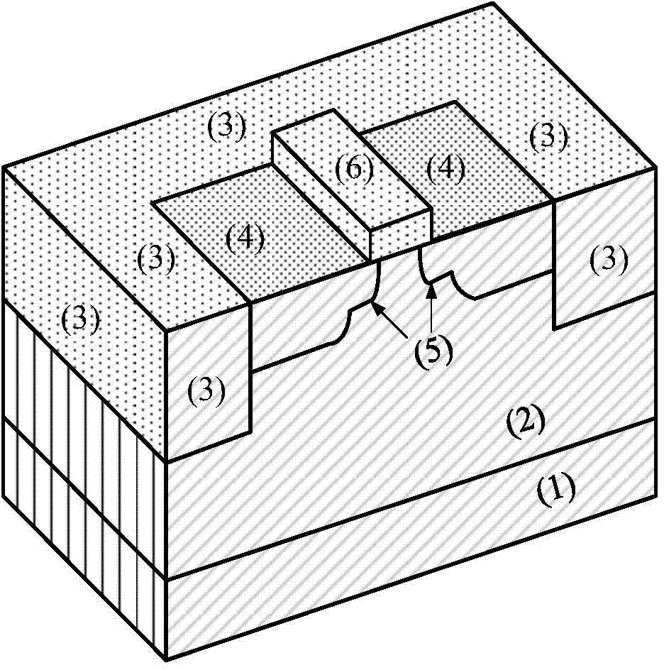
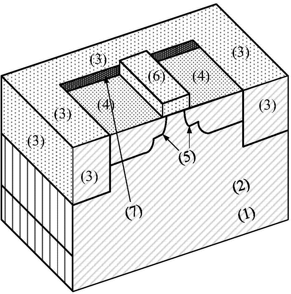
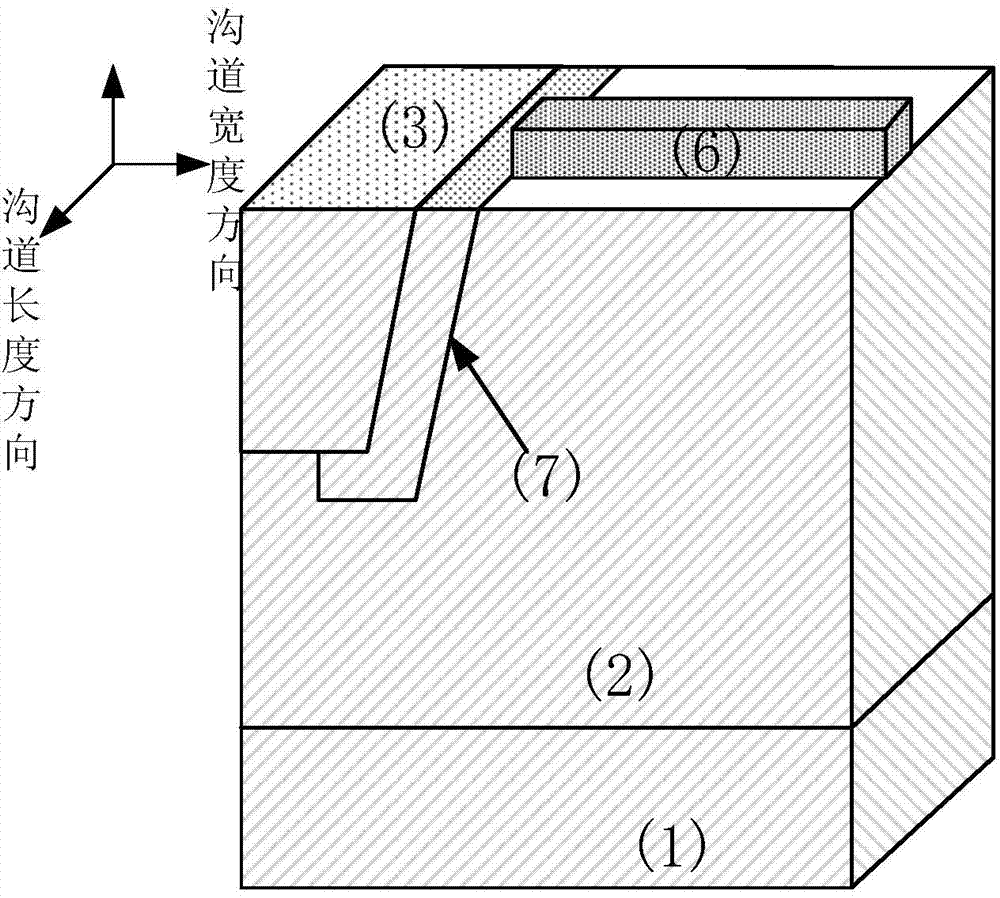
The invention discloses a redundant doping radiation-proof MOS (Metal Oxide Semiconductor) field-effect tube based on a 65nm process, and mainly solves that a traditional 65nm MOS field-effect tube has the problems of threshold voltage drifting, sub-threshold swing degeneration and the degeneration of OFF leakage current under a total dose irradiation environment. The field-effect tube comprises a P-type substrate (1) and epitaxial layers (2) located on a substrate, wherein isolation grooves (3) and grids (6) are respectively arranged all around the upper parts and middle parts of the epitaxial layers, the epitaxial layers between the two side boundaries of a grid and the boundaries in the isolation grooves are internally provided with source and drain active areas (4), and the epitaxial layers below the two side boundaries of the grid are internally provided with light dope source and drain areas (5); a channel is formed in an area between the two light dope source and drain areas (5) is located just below the grid, and a redundant doping areas (7) are inserted in the interfaces of the epitaxial layers at the bottom of the two side isolating grooves which are parallel to the length direction of the channel. According to the MOS field-effect tube provided by the invention, the total dose resistant radiation capacity of devices can be improved, and the field-effect tube can be used for preparing massive integrated circuits.

Description

technical field [0001] The invention belongs to the technical field of semiconductor devices, in particular to a 65nm MOS field-effect transistor resistant to total dose radiation, which can be used in the preparation of large-scale integrated circuits. Background technique [0002] Since the first discovery of the ionizing radiation effect of metal oxide semiconductor field effect transistor MOSFET in 1964, the total dose effect of ionizing radiation has been one of the most important factors leading to functional degradation of electronic system devices and circuits for space applications. The total dose effect refers to the effect that when ionizing radiation particles with energy greater than the forbidden band width of the semiconductor irradiate the semiconductor, some bound state electrons inside the semiconductor absorb the energy of the radiation particles and are excited to the conduction band to generate electron-hole pairs. Studies have shown that the total dose ...

Claims


Application Information

Patent Timeline
Patent Type & Authority Applications(China)
IPC IPC(8): H01L29/78H01L29/06H01L21/336
CPCH01L29/0603H01L29/0688H01L29/66477H01L29/78H01L29/7833
Inventor 刘红侠陈树鹏张丹陈煜海刘永杰王倩琼赵东东王树龙
Owner XIDIAN UNIV
Learn More