Method for bonding conductive geometric structures onto ceramic substrates and resulting components and metamaterials
A technology of conductive geometric structure and ceramic substrate, which is applied in the field of cast sheet-ceramic substrate components and metamaterials, can solve the problems of inability to solve the shape of conductive geometric structure, pollute non-dense ceramic plates, and difficulty in obtaining large thickness, and achieve Reduce the risk of fracturing, avoid sintering deformation, and reduce the effect of sintering shrinkage
- Summary
- Abstract
- Description
- Claims
- Application Information
AI Technical Summary
Problems solved by technology
Method used
Image

Examples
no. 1 example
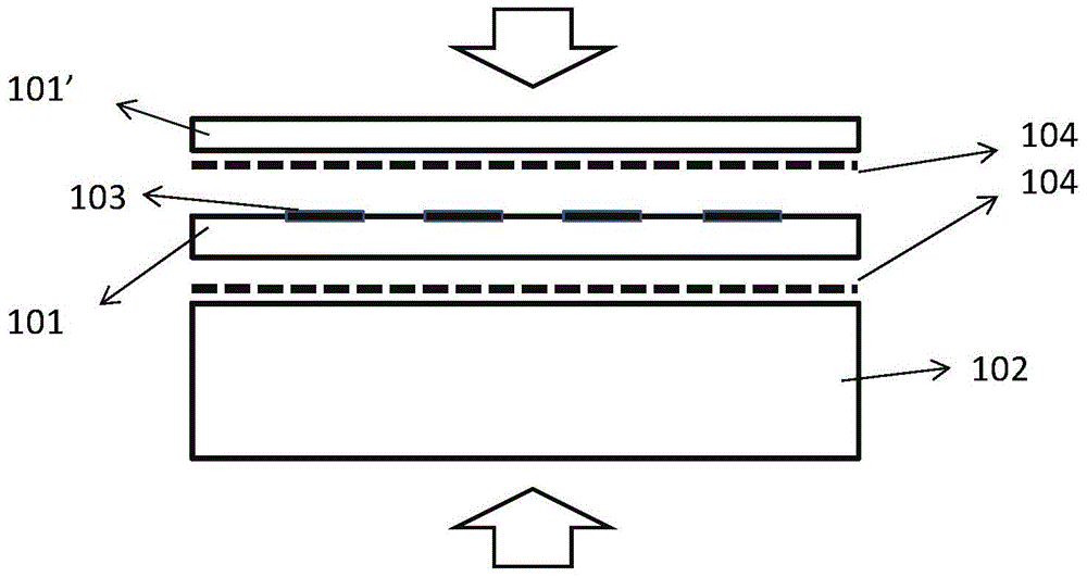
[0077] Such as figure 1 As shown, a planar ceramic substrate 102 is used, the planar ceramic substrate is made of fused silica ceramics by gel injection molding, its porosity is 14%, and the surface is finished to a surface roughness of Ra=0.8. The casting sheets 101, 101' for making green strips contain fused silica powder (average particle size is 3 microns) and dielectric glass powder (available from Beixu Electronics Co., Ltd.), and are made by tape casting, and their thickness is 200 microns . The percentage of glass powder is 15wt% (relative to quartz powder + glass powder).
[0078] Tackifying resin 104 (carbon five petroleum resin, available from Foshan Baolin Chemical Industry Co., Ltd.) is formulated into an organic solution with an organic solvent such as xylene or butanone. Apply the viscous organic solution of the tackifying resin 104 on the surface of the ceramic substrate 102 by spraying, and the thickness after drying is preferably 10-15 microns. Afterwards,...
no. 2 example
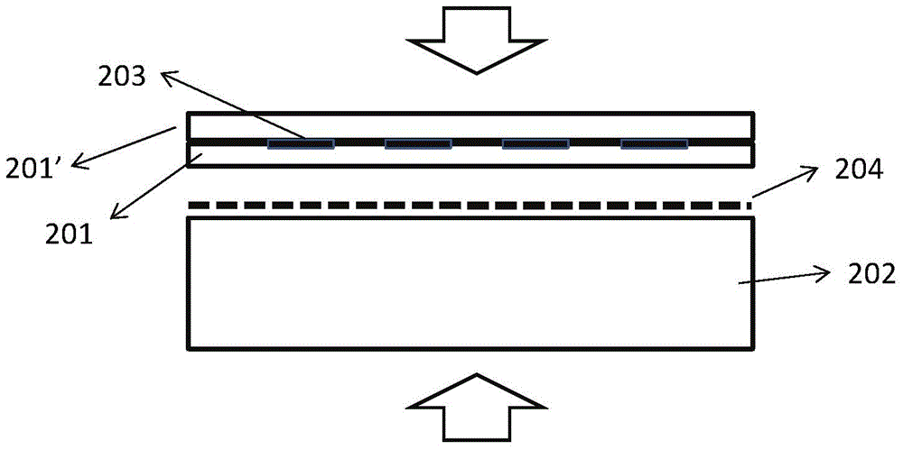
[0082] Such as figure 2 As shown, a planar ceramic substrate 202 is used, the planar ceramic substrate is made of fused silica ceramics by gel injection molding, its porosity is 14%, and the surface is finished to a surface roughness of Ra=0.8. The casting sheets 201, 201' for making the green strips contain fused silica powder (average particle size is 3 microns) and dielectric glass powder (available from Beixu Electronics Co., Ltd.), made by tape casting, and its thickness is 200 microns . The percentage of glass powder is 15wt% (relative to quartz powder + glass powder).
[0083] The difference from the first embodiment is that the silver-based microstructure 203 is screen-printed on the casting sheet 201 first, and then a layer of blank casting sheet 201' is artificially superimposed, and vacuum hot pressing (also called "pre-lamination") The way (pressure 20Mpa, temperature 70 ℃) to produce a double-cast sheet green tape with a conductive geometric structure, high pre...
no. 3 example
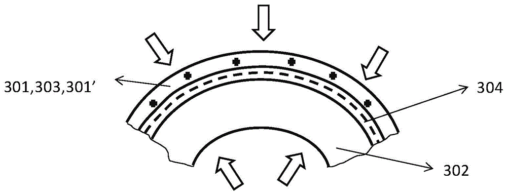
[0088] Such as image 3 As shown, a curved ceramic substrate 302 is used, the curved ceramic substrate is made of fused silica ceramics by gel injection molding, its porosity is 14%, and the surface is finished to a surface roughness of Ra=0.8. The curved ceramic substrate 302 is tile-shaped and has coaxial inner and outer surfaces. The casting sheet 301, 301' for making the green belt contains fused silica powder (average particle size is 3 microns) and dielectric glass powder (available from Beixu Electronics Co., Ltd.), and is made by tape casting, and its thickness is 200 microns . The percentage of glass powder is 15wt% (relative to quartz powder + glass powder).
[0089] First screen-print the silver-based microstructure 303 on the casting sheet 301, then manually superimpose a layer of blank casting sheet 301', and use vacuum hot pressing (also called "pre-pressing") (pressure 20Mpa, temperature 70°C ) to produce a double-cast sheet green tape with a conductive geome...
PUM
| Property | Measurement | Unit |
|---|---|---|
| thickness | aaaaa | aaaaa |
| porosity | aaaaa | aaaaa |
| porosity | aaaaa | aaaaa |
Abstract
Description
Claims
Application Information
 - R&D
- Intellectual Property
- Life Sciences
- Materials
- Tech Scout
- Unparalleled Data Quality
- Higher Quality Content
- 60% Fewer Hallucinations
Browse by: Latest US Patents, China's latest patents, Technical Efficacy Thesaurus, Application Domain, Technology Topic, Popular Technical Reports.
© 2025 PatSnap. All rights reserved.Legal|Privacy policy|Modern Slavery Act Transparency Statement|Sitemap|About US| Contact US: help@patsnap.com