Low temperature polysilicon thin film transistor and its preparation method
A technology of low-temperature polysilicon and thin-film transistors, which is applied in the direction of transistors, semiconductor/solid-state device manufacturing, semiconductor devices, etc., and can solve the problems of reducing the yield rate of thin-film field-effect transistor arrays and unfavorable applications.
- Summary
- Abstract
- Description
- Claims
- Application Information
AI Technical Summary
Problems solved by technology
Method used
Image

Examples
preparation example Construction
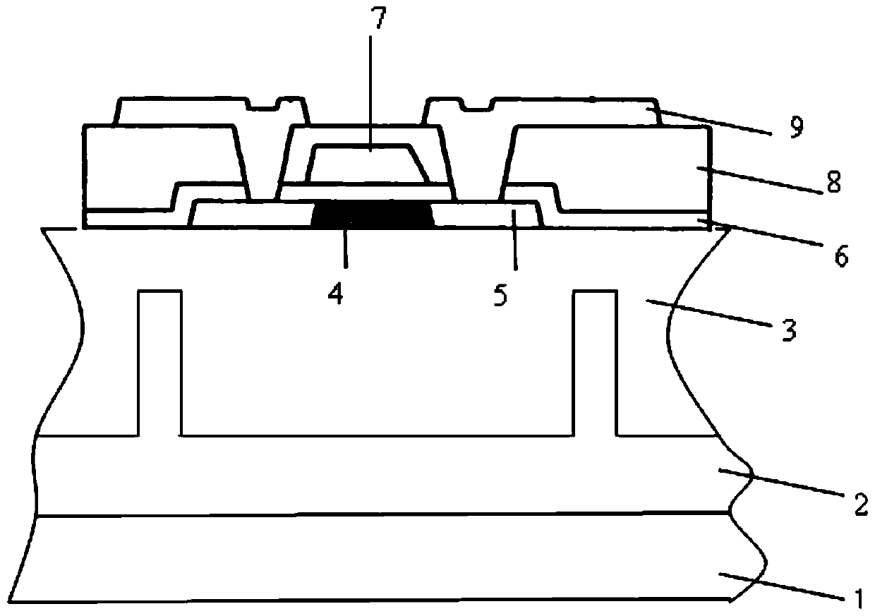
[0065] Correspondingly, the present application also provides a method for preparing a low-temperature polysilicon thin film transistor, comprising the following steps:
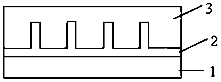
[0066] 1) Depositing a heat conduction layer on the substrate, applying a yellow light process to the heat conduction layer, and thinning the heat conduction layer so that the heat conduction layer has several strip-shaped protrusions;
[0067] 2) depositing a planarization layer on the heat conducting layer having several strip-shaped protrusions;
[0068] 3) Depositing an amorphous silicon layer on the planarization layer, and then performing excimer laser annealing on the amorphous silicon layer to obtain a low-temperature polysilicon film, and then applying a yellow light process to the low-temperature polysilicon film to obtain several The active layer of the active channel; the position of each of the strip-shaped protrusions is outside the corresponding side of the position of each of the active channe...
Embodiment 1
[0097] According to the technical parameters of AMOLED, determine the size of each sub-pixel and the position of TFT inside the sub-pixel.
[0098]Aluminum oxide was deposited using a sputter to deposit a thickness of thermal buffer layer.
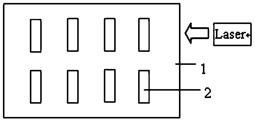
[0099] Through the yellow light process, the heat conduction buffer layer is thinned to form several strip-shaped protrusions; the heat conduction layer pattern is as follows Figure 1 to Figure 3 shown. In the yellow light process, the laser scans from right to left, and the position of each of the strip-shaped protrusions is located on the right side of the position of each of the active channels. The length of each of the strip-shaped protrusions is greater than the corresponding width of each of the active channels, and the width of each of the strip-shaped protrusions is 0.5 μm; the thickness of the heat-conducting buffer layer after thinning is
[0100] SiO deposited by sol-gel method 2 , to deposit a thickness of the planar...
Embodiment 2
[0107] According to the technical parameters of AMOLED, determine the size of each sub-pixel and the position of TFT inside the sub-pixel.
[0108] Silicon carbide is deposited using a sputter to deposit a thickness of thermal buffer layer.
[0109] Through the yellow light process, the heat conduction buffer layer is thinned to form several strip-shaped protrusions; the heat conduction layer pattern is as follows Figure 1 to Figure 3 shown. In the yellow light process, the laser scans from right to left, and the position of each of the strip-shaped protrusions is located on the right side of the position of each of the active channels. The length of each strip-shaped protrusion is greater than the width of each corresponding active channel, and the width of each strip-shaped protrusion is 1 μm; the thickness of the heat-conducting buffer layer after thinning is
[0110] The acrylic material monomer is deposited by spin coating, and then polymerized under UV light, so a...
PUM
| Property | Measurement | Unit |
|---|---|---|
| thickness | aaaaa | aaaaa |
| width | aaaaa | aaaaa |
| width | aaaaa | aaaaa |
Abstract
Description
Claims
Application Information
 - Generate Ideas
- Intellectual Property
- Life Sciences
- Materials
- Tech Scout
- Unparalleled Data Quality
- Higher Quality Content
- 60% Fewer Hallucinations
Browse by: Latest US Patents, China's latest patents, Technical Efficacy Thesaurus, Application Domain, Technology Topic, Popular Technical Reports.
© 2025 PatSnap. All rights reserved.Legal|Privacy policy|Modern Slavery Act Transparency Statement|Sitemap|About US| Contact US: help@patsnap.com