Boron diffusion method for n-type silicon wafer, crystalline silicon solar cell and manufacturing method thereof
A solar cell and diffusion method technology, applied in the field of crystalline silicon solar cells and their fabrication, can solve the problems of increasing the surface recombination rate, being difficult to control, and destroying the surface lattice of silicon wafers, reducing the surface recombination rate and improving the conversion rate. Efficiency, improving the effect of poor uniformity
- Summary
- Abstract
- Description
- Claims
- Application Information
AI Technical Summary
Problems solved by technology
Method used
Image

Examples
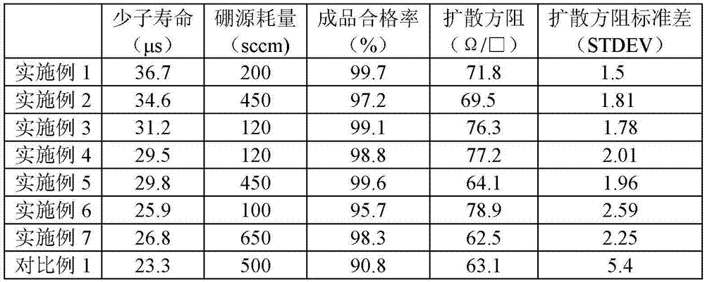
Embodiment 1
[0041] 1) Deposition stage: Take an N-type silicon wafer and carry out phosphorus diffusion and wet etching in sequence, and place the wet-etched silicon wafer (provided by Baoding Tianwei Yingli New Energy Co., Ltd.) in the furnace tube of the diffusion furnace. The silicon wafers are placed perpendicular to the quartz boat, and 500 wafers are placed in each furnace tube. Raise the temperature to 925°C at 10°C / min, feed in nitrogen, oxygen, and nitrogen carrying boron tribromide for reactive deposition for 25 minutes, wherein the oxygen flow rate is 65 sccm, the nitrogen flow rate carrying boron tribromide is 200 sccm, and the nitrogen flow rate is 22.5 slm .
[0042] 2) Diffusion stage: Stop feeding oxygen and boron sources, continue to feed nitrogen gas with a flow rate of 22.5 slm, and at the same time raise the temperature to 960°C at 10°C / min, and surface diffusion at 960°C for 25 minutes.
[0043] 3) Post-oxidation stage: Cool down the silicon wafer to 800°C (cool down...
Embodiment 2
[0046] 1) Deposition stage: Take an N-type silicon wafer and carry out phosphorus diffusion and wet etching in sequence, and place the wet-etched silicon wafer (provided by Baoding Tianwei Yingli New Energy Co., Ltd.) in the furnace tube of the diffusion furnace. The silicon wafers are placed perpendicular to the quartz boat, and 500 wafers are placed in each furnace tube. Raise the temperature to 900°C at 10°C / min, feed nitrogen, oxygen, and nitrogen carrying boron tribromide, wherein the flow rate of oxygen is 160 sccm, the flow rate of nitrogen carrying boron tribromide is 450 sccm, the flow rate of nitrogen gas is 23 slm, and the deposition time is 20 minute.
[0047] 2) Diffusion stage: Stop feeding oxygen and boron sources, continue to feed nitrogen gas with a flow rate of 23 slm, and at the same time raise the temperature to 950°C at 5°C / min, and diffuse on the surface at 950°C for 20 minutes.
[0048] 3) Post-oxidation stage: cool down the silicon wafer to 750°C (the ...
Embodiment 3
[0051] 1) Deposition stage: Take an N-type silicon wafer and carry out phosphorus diffusion and wet etching in sequence, and place the wet-etched silicon wafer (provided by Baoding Tianwei Yingli New Energy Co., Ltd.) in the furnace tube of the diffusion furnace. The silicon wafers are placed perpendicular to the quartz boat, and 500 wafers are placed in each furnace tube. Raise the temperature to 930°C at 10°C / min, feed nitrogen, oxygen, and nitrogen carrying boron tribromide, wherein the flow rate of oxygen is 30 sccm, the flow rate of nitrogen gas carrying boron tribromide is 120 sccm, the flow rate of nitrogen gas is 22 slm, and the deposition time is 30 minute.
[0052] 2) Diffusion stage: Stop feeding oxygen and boron sources, continue to feed nitrogen gas with a flow rate of 24 slm, and at the same time raise the temperature to 1000 °C at 15 °C / min, and diffuse on the surface at 1000 °C for 30 minutes.
[0053] 3) Post-oxidation stage: Cool down the silicon wafer to 85...
PUM
 Abstract
Description
Claims
Application Information
 - R&D
- Intellectual Property
- Life Sciences
- Materials
- Tech Scout
- Unparalleled Data Quality
- Higher Quality Content
- 60% Fewer Hallucinations
Browse by: Latest US Patents, China's latest patents, Technical Efficacy Thesaurus, Application Domain, Technology Topic, Popular Technical Reports.
© 2025 PatSnap. All rights reserved.Legal|Privacy policy|Modern Slavery Act Transparency Statement|Sitemap|About US| Contact US: help@patsnap.com