Semiconductor memory device
a memory device and semiconductor technology, applied in the direction of information storage, static storage, digital storage, etc., can solve the problems of inability to perform stable reading and writing with a low power supply voltage, prone to write data (inversion of held data), and low noise margins, so as to achieve stable writing and reading and increase current consumption
- Summary
- Abstract
- Description
- Claims
- Application Information
AI Technical Summary
Benefits of technology
Problems solved by technology
Method used
Image
Examples
first embodiment
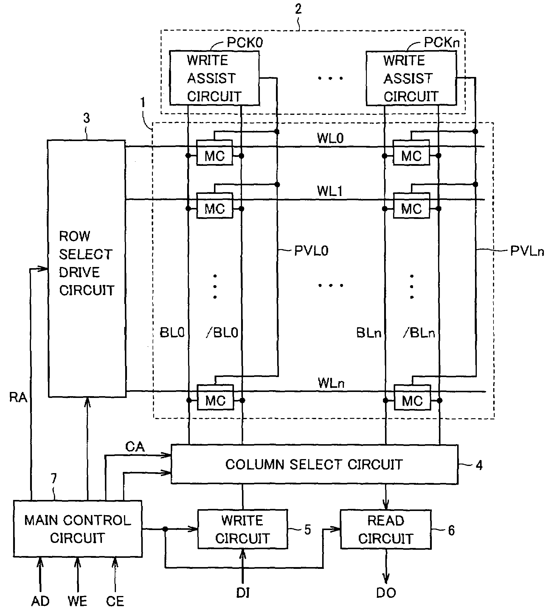
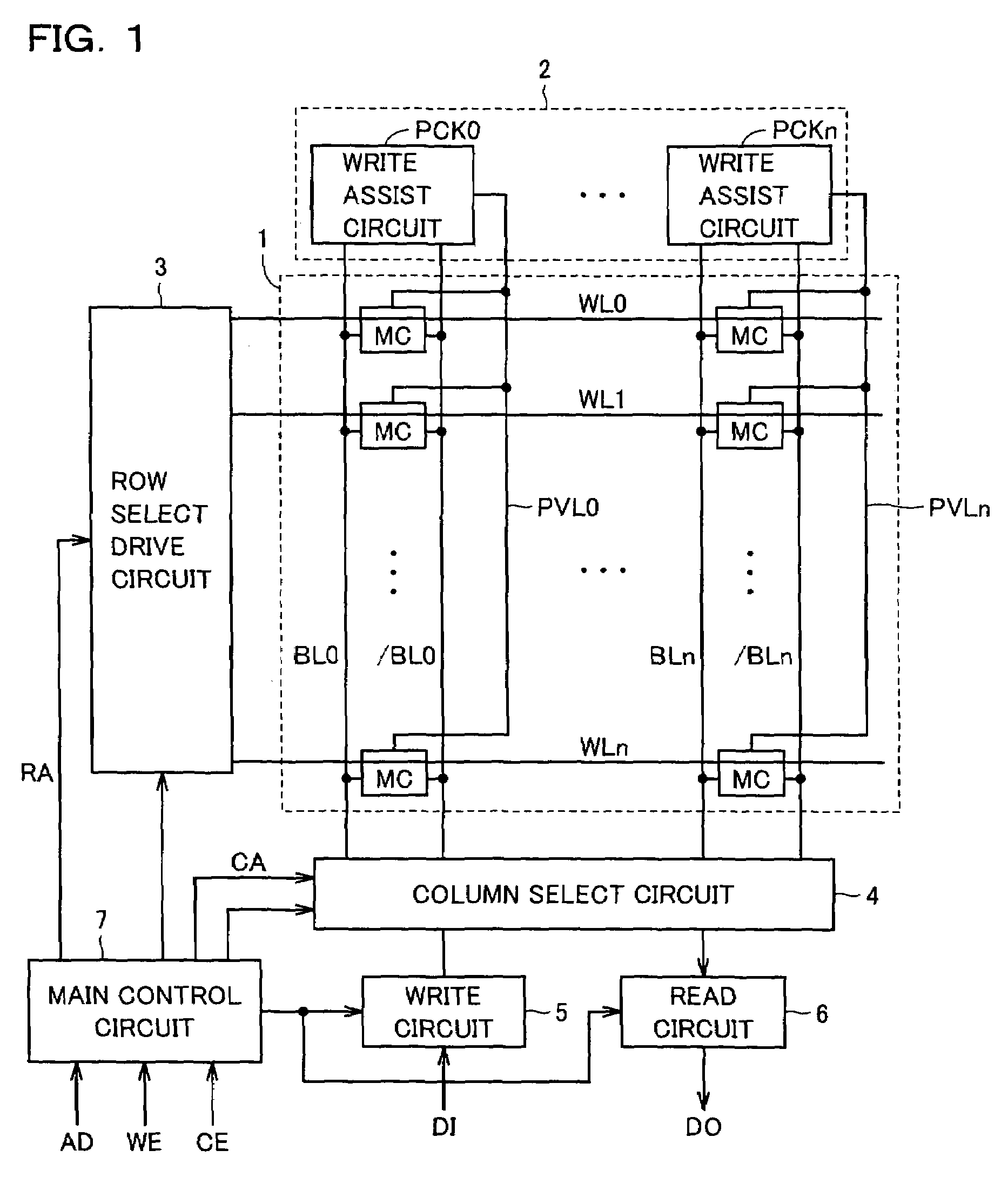
[0107]FIG. 4 shows a construction of the write assist circuit according to the first embodiment of the invention. FIG. 4 shows a construction of the write assist circuit provided for one bit line pair BL and / BL. In FIG. 4, memory cells MC in one column are connected to a common bit line pair BL and / BL. A high-side power supply line (which will be referred to as a “VDD source line” hereinafter) VDM transmitting high-side power supply voltage VDD is arranged as the cell power supply line for bit line pair BL and / BL. VDD source line VDM is connected to high-side power supply nodes VH of memory cells MC on the corresponding column.
[0108]The write assist circuits include write assist circuits PCKa and PCKb arranged at opposite ends of VDD source line VDM, respectively. Write assist circuits PCKa and PCKb have the same circuit construction, and corresponding portions are allotted with the same reference numerals.
[0109]Write assist circuit PCKa includes an inverter IV1 receiving a volta...
second embodiment
[0141]FIG. 8 schematically shows a construction of a portion (memory cell circuit) related to memory cells MC in one row of a semiconductor memory device according to a second embodiment of the invention. In the construction shown in FIG. 8, write assist circuits PCKa and PCKb are arranged on the opposite sides of VDD source line VDM. VDD source line VDM is individually arranged for each column, and is commonly coupled to high-side power supply nodes VH of memory cells MC arranged in alignment in the corresponding column. In FIG. 8, memory cells MC arranged in four rows are shown as a representative example. Word lines WL0-WL3 are arranged corresponding to the respective memory cell rows.
[0142]Bit lines BL and / BL are arranged corresponding to the memory cell column, and bit lines BL and / BL are coupled to an internal data bus IO via column select gate CSG. Column select gate CSG is selectively made conductive to couple corresponding bit lines BL and / BL to internal data bus IO acco...
third embodiment
[0157]FIG. 10 schematically shows a construction of a memory cell array of the semiconductor memory device according to a third embodiment of the invention. FIG. 10 schematically shows a circuit construction for memory cells MC arranged in four rows and four columns. Bit line pairs BL0 and / BL0, BL1 and / BL1, BL2 and / BL2, and BL3 and / BL3 are arranged corresponding to the memory cell columns, respectively.
[0158]Bit lines BL0 and / BL0, and BL1 and / BL1 are coupled to a two-to-one selector 4b0, and bit lines BL2 and / BL2, and BL3 and / BL3 are likewise coupled to a two-to-one selector 4b1. These two-to-one selectors 4b0 and 4b1 perform two-to-one selection according to column address signal CA, and each selects one bit line pair from the corresponding two bit line pairs.
[0159]A write driver 5a0 and a sense amplifier circuit 6a0 are arranged for two-to-one selector 4b0, and a write driver 5a1 and a sense amplifier circuit 6a1 are arranged for two-to-one selector 4b1.
[0160]These two-to-...
PUM
 Abstract
Description
Claims
Application Information
 - R&D
- Intellectual Property
- Life Sciences
- Materials
- Tech Scout
- Unparalleled Data Quality
- Higher Quality Content
- 60% Fewer Hallucinations
Browse by: Latest US Patents, China's latest patents, Technical Efficacy Thesaurus, Application Domain, Technology Topic, Popular Technical Reports.
© 2025 PatSnap. All rights reserved.Legal|Privacy policy|Modern Slavery Act Transparency Statement|Sitemap|About US| Contact US: help@patsnap.com


