A kind of nanocomposite cr-al-o solar spectrum selective absorption coating and its preparation method
A solar spectrum and selective absorption technology, applied in the field of nanocomposite Cr-Al-O solar spectrum selective absorption coating and its preparation, can solve the problem of less research on the optical properties and microstructure of the coating, high ion energy and low cost and other problems, to achieve the effect of good industrial application prospects, simple equipment structure, and overcoming poor adhesion.
- Summary
- Abstract
- Description
- Claims
- Application Information
AI Technical Summary
Problems solved by technology
Method used
Image
Examples
preparation example Construction
[0038] The preparation process of this embodiment is:
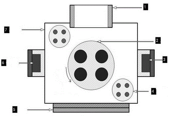
[0039] First, the cleaning of the base material. The base material was ultrasonically cleaned in acetone, alcohol, and deionized water for 15 minutes, then dried in a desiccator, and then loaded on a workpiece rack whose rotation speed could be adjusted between 3-5 rpm, and the sample preparation chamber door was closed.
[0040] Second, the acquisition of a vacuum environment. The first is to use a mechanical pump for pumping under low vacuum conditions; when the vacuum reaches below 2pa, turn on the molecular pump to convert the pumping system to a high vacuum acquisition system until 8×10 -3 Below pa.
[0041] Third, the preparation of the coating. First, set the rotation speed of the workpiece holder to 3-5 rpm. Then, high-power (1.4-1.6 kilowatts) arc discharge technology is used to evaporate Cr ions from the Cr target with electric current, and deposit them on a rotating substrate connected to a negative bias of -800 to...
Embodiment 1
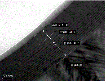
[0043] Example 1: At 10 -3 Under the vacuum degree, control the speed to 3rpm, use the high-energy ions evaporated from the Cr target to deposit the Cr layer on the cleaned stainless steel substrate. The power of the deposition source is 1.4 kilowatts, the bias voltage on the workpiece is -800V, and the deposition time is 10min. The thickness of the infrared high reflection layer is 500 nanometers; after the deposition, the bias voltage is reduced to -100V, oxygen gas with a flow rate of 15SCCM is introduced, and the argon flow rate is adjusted to make the vacuum degree 0.4Pa, and the CrAl target is turned on, the current is 30A, The corresponding power is 0.6 kilowatts. The low-oxygen absorption layer is deposited. The low-oxygen absorption layer is composed of Cr-Al alloy nanocrystalline and amorphous phase (Al 2 Cr)-O X The deposition time of the composite material is 2min, where X is 0.67, the thickness is 65 nanometers, and the size of the metal nanocrystal is 4-5 nanometers...
Embodiment 2
[0044] Example 2: At 10 -2 Under the vacuum degree, control the rotation speed to 5rpm, use the high-energy ions evaporated from the Cr target to deposit the Cr layer on the cleaned stainless steel substrate. The power of the deposition source is 1.6 kW, the bias voltage on the workpiece is -1000V, and the deposition time is 10min. The thickness of the infrared high reflection layer is 600 nanometers; after the deposition is completed, the bias voltage is reduced to -200V, oxygen gas with a flow rate of 20SCCM is introduced, and the argon flow rate is adjusted to make the vacuum degree 0.5Pa. The CrAl target is turned on and the current is 40A. The corresponding power is 0.8 kilowatts, and the low oxygen absorption layer is deposited. The low oxygen absorption layer is composed of Cr-Al alloy nanocrystalline and amorphous phase (Al 2 Cr)-O X The deposition time of the composite material is 2min, where X is 0.7, the thickness is 70 nanometers, and the size of the metal nanocrystal...
PUM
| Property | Measurement | Unit |
|---|---|---|
| thickness | aaaaa | aaaaa |
| thickness | aaaaa | aaaaa |
| thickness | aaaaa | aaaaa |
Abstract
Description
Claims
Application Information
 - R&D Engineer
- R&D Manager
- IP Professional
- Industry Leading Data Capabilities
- Powerful AI technology
- Patent DNA Extraction
Browse by: Latest US Patents, China's latest patents, Technical Efficacy Thesaurus, Application Domain, Technology Topic, Popular Technical Reports.
© 2024 PatSnap. All rights reserved.Legal|Privacy policy|Modern Slavery Act Transparency Statement|Sitemap|About US| Contact US: help@patsnap.com


