Alignment device and alignment method for lithography equipment

An alignment device and alignment mark technology, applied in the field of photolithography, can solve the problems of complex optical path structure, high requirements for wedge plate group processing, manufacturing, assembly and adjustment, and engineering difficulty, so as to reduce the influence of crosstalk and increase energy. Effectiveness of utilization and improved alignment accuracy

Active Publication Date: 2013-01-23
SHANGHAI MICRO ELECTRONICS EQUIP (GRP) CO LTD +1
View PDF7 Cites 5 Cited by
  • Summary
  • Abstract
  • Description
  • Claims
  • Application Information

AI Technical Summary

Problems solved by technology

[0008] However, when using a wedge array, the requirements for the surface shape and wedge angle consistency of the two wedges with the same positive and negative orders of refraction are very high; and the requirements for the manufacturing, assembly and adjustment of the wedge plate group are also very high. It is difficult and expensive to realize the project
[0009] Another prior art situation (see (2) Chinese invention patent, publication number: 200710044152.1, title of invention: an alignment system for lithography equipment), the alignment system uses a three-period phase The grating only uses the first-order diffracted light of these three periods as the alignment signal, which can achieve a large capture range and high alignment accuracy, and only uses the first-order diffracted light of each period to obtain a stronger signal strength , improve the signal-to-noise ratio of the system, and do not need to use adjustment devices such as wedges to separate multi-channel high-order diffraction components, simplifying the optical path design and debugging difficulty, but the alignment marks in the alignment system are lined up on the silicon wafer and the reference board distribution, which reduces the utilization rate of the light source, and this arrangement mode scans the corresponding reference grating when each group of grating images of the alignment mark scans the corresponding reference grating, and the grating images of different periods scan a reference grating at the same time, which will cause the scanning signal. Crosstalk problem, which is not conducive to the alignment of lithography equipment
[0010] The optical paths of the above two existing technologies are complicated in structure and relatively bulky, occupying a considerable part of the space of the lithography machine, and difficult to install and adjust

Method used


Image

  • Alignment device and alignment method for lithography equipment
  • Alignment device and alignment method for lithography equipment
  • Alignment device and alignment method for lithography equipment

Examples


Embodiment Construction

[0046] In the following, preferred embodiments according to the present invention will be described in detail with reference to the accompanying drawings. For the convenience of describing and highlighting the present invention, relevant components existing in the prior art are omitted from the drawings, and the description of these known components will be omitted.

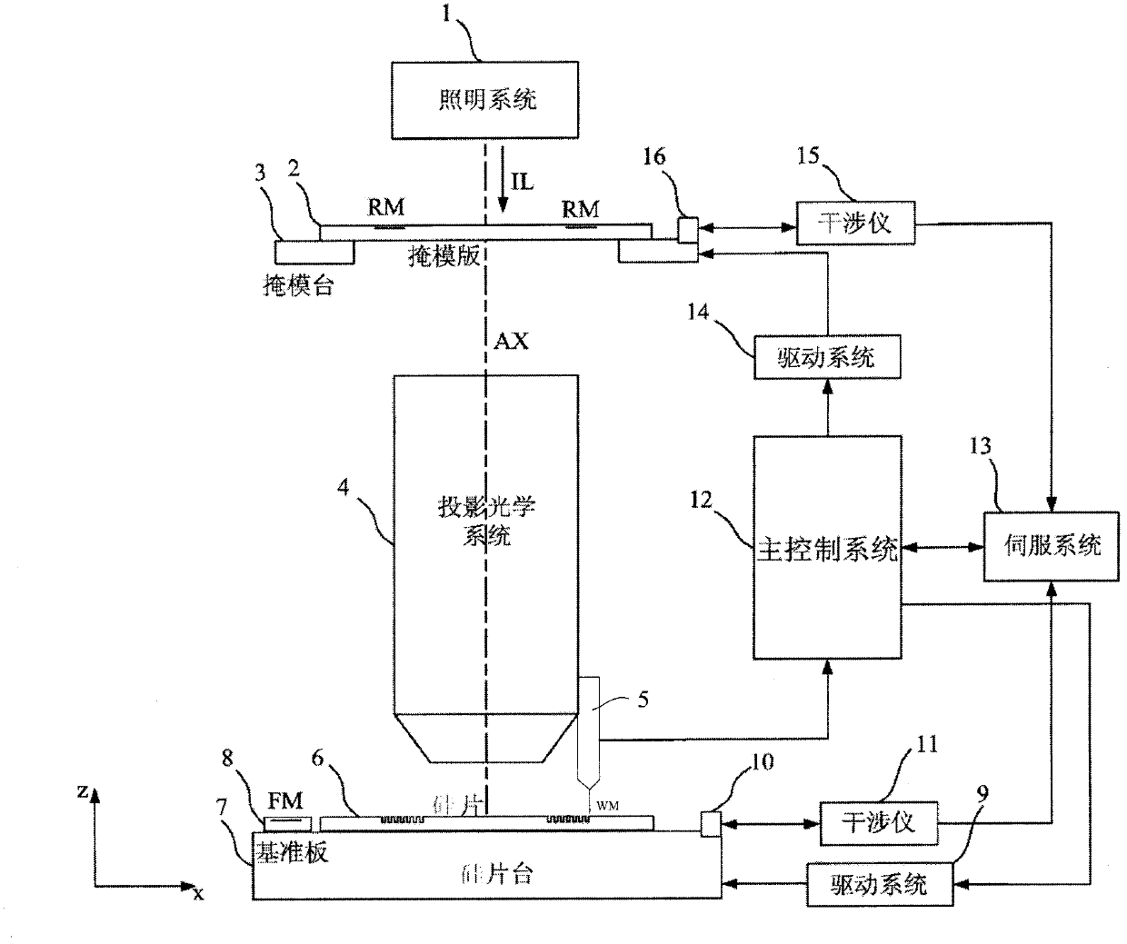
[0047] figure 1 Shown is a schematic structural view of a lithography apparatus using the alignment device according to the present invention. The composition of the lithographic apparatus includes: an illumination system 1 for providing an exposure beam; a mask holder and a mask table 3 for supporting a reticle 2 with a mask pattern and alignment marks with a periodic structure RM; a projection optical system 4 for projecting the mask pattern on the reticle 2 onto the wafer 6; a wafer holder for supporting the wafer 6 and a wafer stage 7 with fiducial marks engraved on the wafer stage 7 FM reference plate 8, a...


PUM


Abstract

An alignment device comprises a light source, a transmission optical fiber, a shaping lens group, an integrator, a beam expander lens group, an alignment optical fiber, a photoelectric detector and a signal processing system. Light emitted from the light source passes through the transmission optical fiber and the shaping lens group and is converted into a parallel light beam; the parallel light beam is converted by the integrator into a light beam with uniformly distributed energy; the beam expander lens group changes the diameter of the light beam to be equivalent to the diameter of a core of the alignment optical fiber; the light beam is coupled to the alignment optical fiber; the light beam emitted from the alignment optical fiber irradiates on an alignment mark; the light emitted from the alignment mark passes through the photoelectric detector, a light signal is converted into an electric signal, and the position information of the alignment mark is obtained by the signal processing system through calculation.

Description

technical field [0001] The invention relates to the field of lithography, and in particular to an alignment device and an alignment method for lithography equipment. Background technique [0002] The lithography equipment in the prior art is mainly used in the manufacture of integrated circuits (ICs) or other micro devices. Through photolithography equipment, multi-layer masks with different mask patterns are sequentially exposed and imaged on a silicon wafer coated with photoresist under precise alignment. The current lithography equipment is roughly divided into two categories, one is stepping lithography equipment, the mask pattern is exposed and imaged on one exposure area of ​​the silicon wafer, and then the silicon wafer moves relative to the mask to move the next exposure area Go to the mask pattern and under the projection objective lens, again expose the mask pattern on another exposed area of ​​the silicon wafer, and repeat this process until all exposed areas on ...

Claims


Application Information

Patent Timeline
Patent Type & Authority Applications(China)
IPC IPC(8): G03F9/00G03F7/20
Inventor 杜聚有朱婧怡徐荣伟
Owner SHANGHAI MICRO ELECTRONICS EQUIP (GRP) CO LTD
Why Eureka
Try Eureka