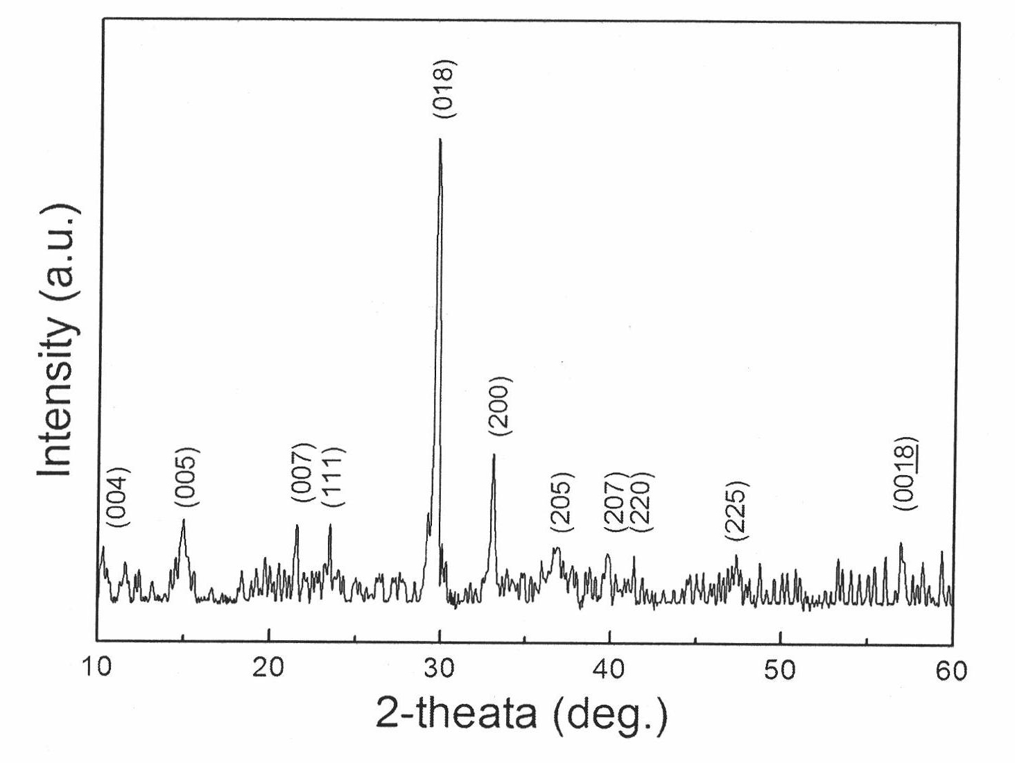
Preparation method of Bi3TiNbO9-Bi4Ti3O12 natural superlattice ferroelectric film on Si substrate
A bi3tinbo9-bi4ti3o12, ferroelectric thin film technology, applied in the field of information functional thin film materials, can solve the problems of unseen natural superlattice ferroelectric thin films, complex process, expensive equipment, etc., and achieve easy large-area film formation and component control Precise, highly uniform results
- Summary
- Abstract
- Description
- Claims
- Application Information
AI Technical Summary
Problems solved by technology
Method used
Image
Examples
Embodiment 1
[0042] (1) Select a p-type single crystal Si substrate with a resistivity of 3Ω cm and a (100) crystal orientation as the substrate, and perform surface treatment and cleaning according to the requirements of the semiconductor plane process;
[0043] (2) adopt the following raw materials (its purity is analytically pure 99.99%) to prepare Bi 3 TiNbO 9 -Bi 4 Ti 3 o 12 Sol:
[0044]
[0045] Among them: (a) bismuth nitrate (Bi(NO 3 ) 3 ·5H 2 O), niobium ethoxide (Nb(OC 2 h 5 ) 5 ), butyl titanate (C 16 h 36 o 4 The molar ratio of Ti) is 7.35: 1.00: 4.00; (b) solvent ethylene glycol methyl ether (C 3 h 8 o 2 ), catalyst glacial acetic acid (CH 3 COOH) and stabilizer acetylacetone (CH 3 COCH 2 COCH 3 ) are respectively 35.00%: 12.00%: 46.20% by volume; (c) 6.17 moles (a) solute raw material (which contains: 3.67 moles of bismuth nitrate, 0.50 moles of niobium ethoxide, 2.00 moles of butyl titanate) with 93.20ml ( b) Solvent, catalyst, stabilizer raw material...
Embodiment 2
[0064] Embodiment 2: (the purity of each raw material is required to be more than 99.99% of analytical purity)
[0065] (1) Use a resistivity of 5 Ω cm, (100) crystal orientation p-type single crystal Si substrate as the substrate, and perform surface treatment and cleaning according to the requirements of the semiconductor plane process;
[0066] (2) adopt the following raw materials (its purity is analytically pure 99.99%) to prepare Bi 3 TiNbO 9 -Bi 4 Ti 3 o 12 Sol:
[0067]
[0068] Among them: (a) bismuth nitrate (Bi(NO 3 ) 3 ·5H 2 O), niobium ethoxide (Nb(OC 2 h 5 ) 5 ), butyl titanate (C 16 h 36 o 4 The molar ratio of Ti) is 7.28: 1.00: 4.00; (b) solvent ethylene glycol methyl ether (C 3 h 8 o 2 ), catalyst glacial acetic acid (CH 3 COOH) and stabilizer acetylacetone (CH 3 COCH 2 COCH 3 ) are respectively 45.00%: 18.00%: 30.20% by volume; (c) 6.14 moles of (a) solute raw material (which contains: 3.64 moles of bismuth nitrate, 0.50 moles of niobiu...
Embodiment 3
[0075] Embodiment 3: (each raw material purity all requires to be more than 99.99% of analytical purity)
[0076] (1) The resistivity is 10Ω·cm, and the (100) crystal orientation p-type single crystal Si substrate is used as the substrate, and the surface is treated and cleaned according to the requirements of the semiconductor planar process;
[0077] (2) adopt the following raw materials (its purity is analytically pure 99.99%) to prepare Bi 3 TiNbO 9 -Bi 4 Ti 3 o 12 Sol:
[0078]
[0079] Among them: (a) bismuth nitrate (Bi(NO 3 ) 3 ·5H 2 O), niobium ethoxide (Nb(OC 2 h 5 ) 5 ), butyl titanate (C 16 h 36 o 4 The molar ratio of Ti) is 7.21: 1.00: 4.00; (b) solvent ethylene glycol methyl ether (C 3 h 8 o 2 ), catalyst glacial acetic acid (CH 3 COOH) and stabilizer acetylacetone (CH 3 COCH 2 COCH 3 ) are respectively 55.00%: 18.00%: 20.20% by volume; (c) 6.10 moles of (a) solute raw material (which contains: 3.60 moles of bismuth nitrate, 0.50 moles of n...
PUM
| Property | Measurement | Unit |
|---|---|---|
| thickness | aaaaa | aaaaa |
| thickness | aaaaa | aaaaa |
| thickness | aaaaa | aaaaa |
Abstract
Description
Claims
Application Information
 - Generate Ideas
- Intellectual Property
- Life Sciences
- Materials
- Tech Scout
- Unparalleled Data Quality
- Higher Quality Content
- 60% Fewer Hallucinations
Browse by: Latest US Patents, China's latest patents, Technical Efficacy Thesaurus, Application Domain, Technology Topic, Popular Technical Reports.
© 2025 PatSnap. All rights reserved.Legal|Privacy policy|Modern Slavery Act Transparency Statement|Sitemap|About US| Contact US: help@patsnap.com


