


Quick Research
Generate reliable direction feasibility study reports for your R&D in just a few steps.

Technical Q&A
Discover and master advanced knowledge NOW. Basics, ideas, possibilities, all at once.

Find Solutions
As an expert in R&D theories, this can generate solutions to your technical problems instantly.

Evaluate Feasibility
Analyze your overall solution with one click, know your potential R&D risks in advance.

Monitor Landscape
Get weekly tech updates, stay abreast of the latest tech innovations and key insights.
Polarized tuning ferroelectric film diode memory
A ferroelectric thin film and diode technology, applied in the field of microelectronics, can solve problems such as restricting the development of flash memory, and achieve the effects of improving programming/erasing speed, fast reading and writing speed, and good retention characteristics
- Summary
- Abstract
- Description
- Claims
- Application Information
AI Technical Summary
Problems solved by technology
Method used
Image

Examples
Embodiment Construction
[0022] The principles and features of the present invention are described in conjunction with the following drawings, and the examples are only used to explain the present invention, and are not used to limit the material scope of the present invention.
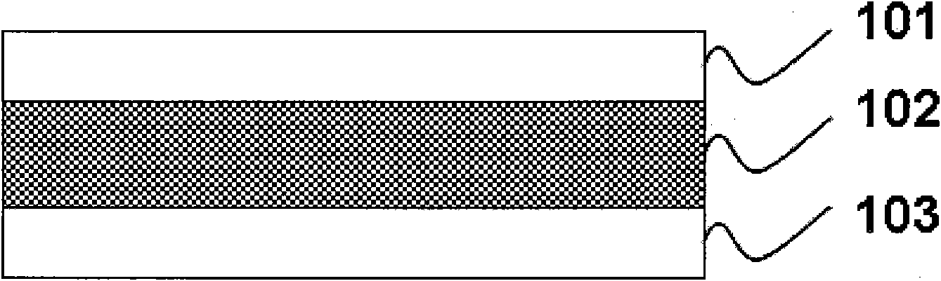
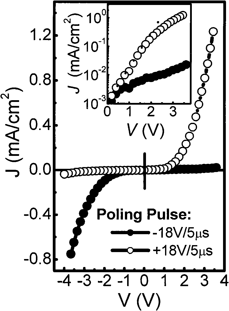
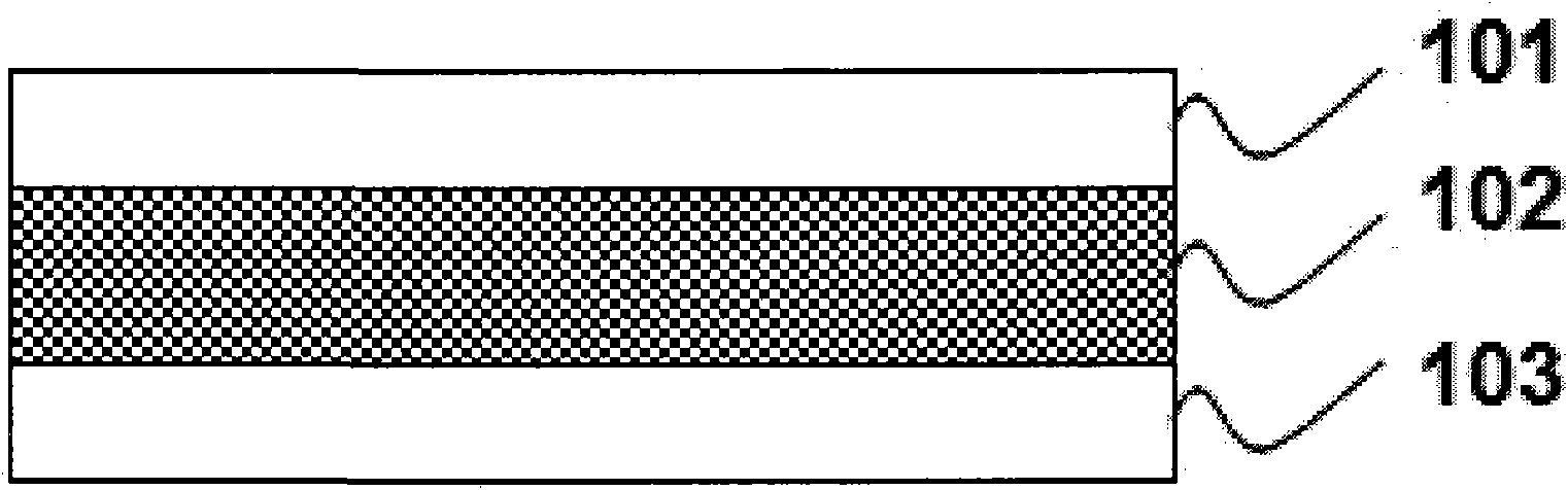
[0023] This example tunes a ferroelectric thin film diode memory storage cell such as figure 1 As shown, it includes a substrate and a lower electrode 103 (strontium ruthenate / strontium titanate), bismuth ferrite 102, and an upper electrode (Pt, Au) 101.
[0024] The above device is prepared by the following method:
[0025] 1. With the (100) direction single-crystal strontium titanate as the substrate, grow the bottom electrode of strontium ruthenate (with a thickness of 50nm-150nm) by pulsed laser deposition (PLD).
[0026] 2. On the above substrate, deposit bismuth ferrite (with a thickness of 200nm-500nm) by PLD.
[0027] 3. Using DC magnetron sputtering to grow a platinum metal upper electrode (thickness 100nm-150nm). ...
PUM
| Property | Measurement | Unit |
|---|---|---|
| Thickness | aaaaa | aaaaa |
| Thickness | aaaaa | aaaaa |
| Thickness | aaaaa | aaaaa |
Abstract
Description
Claims
Application Information
 - R&D Engineer
- R&D Manager
- IP Professional
- Industry Leading Data Capabilities
- Powerful AI technology
- Patent DNA Extraction
Browse by: Latest US Patents, China's latest patents, Technical Efficacy Thesaurus, Application Domain, Technology Topic, Popular Technical Reports.
© 2024 PatSnap. All rights reserved.Legal|Privacy policy|Modern Slavery Act Transparency Statement|Sitemap|About US| Contact US: help@patsnap.com