
Low cost high density rectifier matrix memory

a rectifier matrix and high density technology, applied in semiconductor/solid-state device testing/measurement, instruments, etc., can solve the problems of high storage cost and high cost of flash memory, and achieve the effect of low cost, low testing cost and low cos

Inactive Publication Date: 2005-10-18
WESTERN DIGITAL TECH INC
View PDF2 Cites 37 Cited by
  • Summary
  • Abstract
  • Description
  • Claims
  • Application Information

AI Technical Summary

Benefits of technology

[0012]The present invention is a means for constructing a high density rectifier matrices (as might be used to construct electronic memory) such that the costs are kept low. By constructing memory devices in three dimensions and integrating simple test circuitry that can rapidly verify the operation of such devices, storage densities can be made very high while keeping testing time (and the associated costs of testing) very low. It is believed that memory devices can be manufactured which will be dramatically lower cost than current technologies.
[0013]The present invention also offers advantages over existing technology in that this memory technology could be added to a variety of existing semiconductor devices. Also, a one time programmable variation of the device could be created with little additional effort.
[0014]Finally, the present invention also offers advantages over existing technology in that this memory technology, by virtue of its exceptionally simple design, will retain its cost savings even when manufactured three-dimensionally in layers.

Problems solved by technology

Many storage solutions, such as FLASH memory (a non-volatile, rewritable memory technology), are currently very expensive.
This is because FLASH is so expensive that rather than have many FLASH memory devices, users will typically own very few FLASH memory devices which they will reuse depending on their current needs.

Method used


Image

  • Low cost high density rectifier matrix memory
  • Low cost high density rectifier matrix memory
  • Low cost high density rectifier matrix memory

Examples


Embodiment Construction

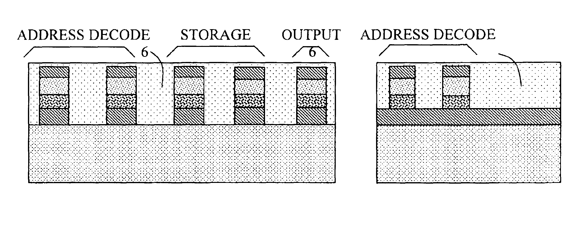
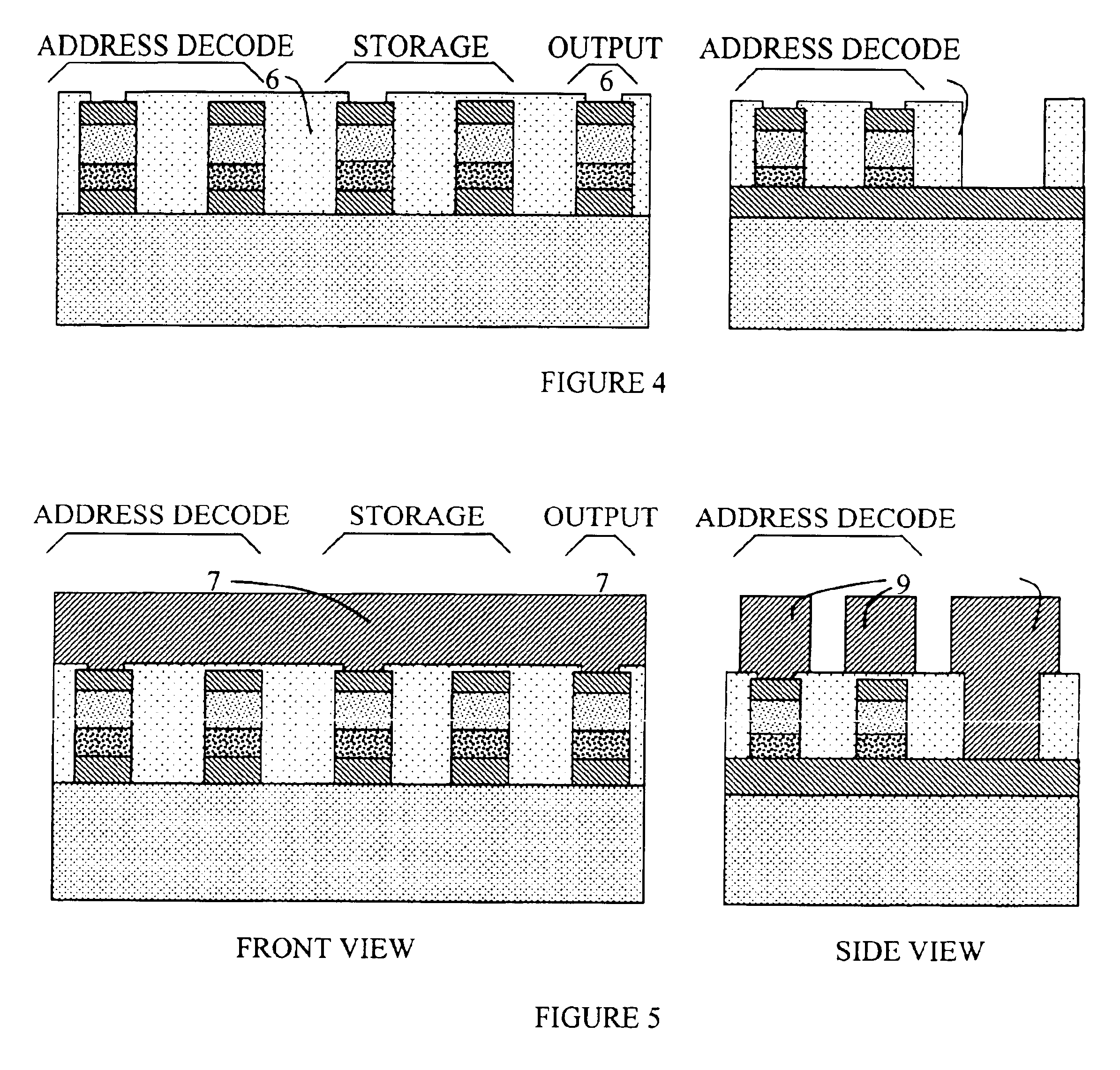
[0022]The present invention is a means for fabricating semiconductor memory in three dimensions. This memory will be fabricated using a process similar to that used to construct Thin Film Transistor (TFT) flat panel displays—in particular, using deposited semiconductor material on insulating substrates.

[0023]Refer now to the figures which show a preferred embodiment of the invention. FIG. 1 shows a possible configuration of a prepared substrate. This substrate consists of a base (1) that is typically made of glass, of Silicon Dioxide on a silicon wafer, or of other insulating material. On top of this is deposited about 1000 Å of metal (2) such as TiAu (Ti-gold), Ni (Nickel), or Al (Aluminum). Next is deposited 250 Å of N+ amorphous Silicon (N+αSi:H) (3) followed by 1000 Å of αSi:H (4). Finally, 100 Å of metal (5) is deposited. It should be noted that the metals and the thicknesses are not critical, so long as certain functional requirements are met. Bottom metal (2) can be made of a...


PUM


Abstract

A high density memory device is fabricated three dimensionally in layers. To keep points of failure low, address decoding circuits are included within each layer so that, in addition to power and data lines, only the address signal lines need be interconnected between the layers.

Description

CROSS REFERENCE TO RELATED PROVISIONAL APPLICATION[0001]The present patent application claims priority to provisional patent application 60 / 213,419 titled “LOW COST HIGH DENSITY RECTIFIER MATRIX MEMORY” which was filed on Jun. 22, 2000 and which is hereby incorporated by reference.CROSS-REFERENCE TO RELATED PATENTS[0002]This application makes references to U.S. Pat. No. 5,889,694 for a “Dual-Addressed Rectifier Storage Device” issued March 1999, to U.S. Pat. No. 3,245,051 for “Information Storage Matrices” issued April 1996, and those patents are hereby incorporated herein by reference.BACKGROUND OF THE INVENTION[0003]1. Field of invention[0004]The present invention relates to semiconductor storage devices, and more particularly to low cost memory resulting from manufacturing efficiencies which construct the devices in three-dimensions and which incorporate efficient testing mechanisms.[0005]2. Description of Prior Art[0006]Many versions of three-dimensional memory arrays have been ...

Claims


Application Information

Patent Timeline
Patent Type & Authority Patents(United States)
IPC IPC(8): H01L21/70G11C29/02H01L27/12H01L27/10H01L21/84
CPCG11C5/025G11C29/006G11C29/02G11C29/025H01L21/84H01L22/32H01L27/10H01L27/105H01L27/12H01L27/1052G11C16/04H01L2924/0002G11C2029/5006H01L2924/00G11C5/02G11C7/00G06K5/04H10B99/00
Inventor SHEPARD, DANIEL ROBERT
Owner WESTERN DIGITAL TECH INC
Learn More