Lithography method
A lithography and patterning technology, applied in optics, optomechanical equipment, instruments, etc., can solve the problems of resist pattern collapse, reduction, and low production volume
- Summary
- Abstract
- Description
- Claims
- Application Information
AI Technical Summary
Problems solved by technology
Method used
Image

Examples
Embodiment Construction
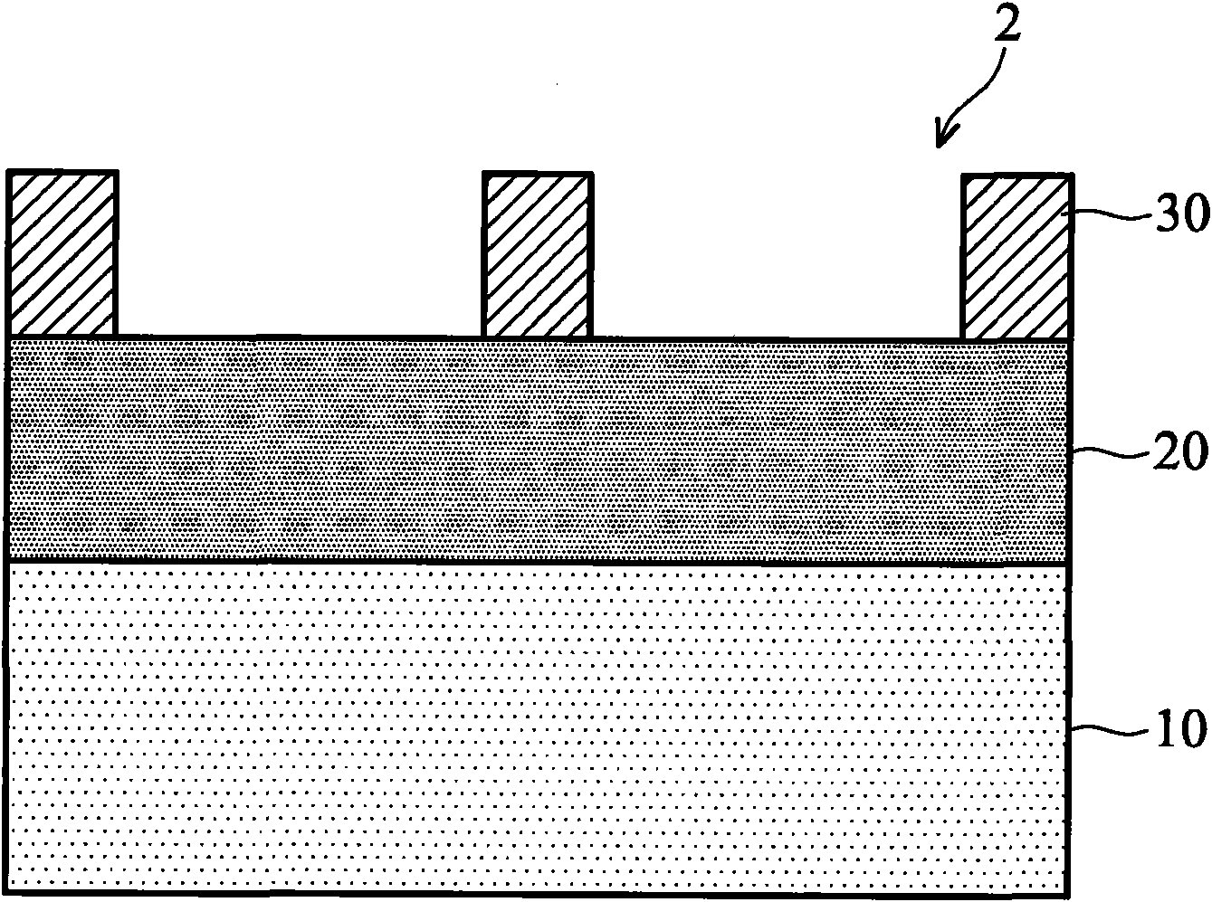
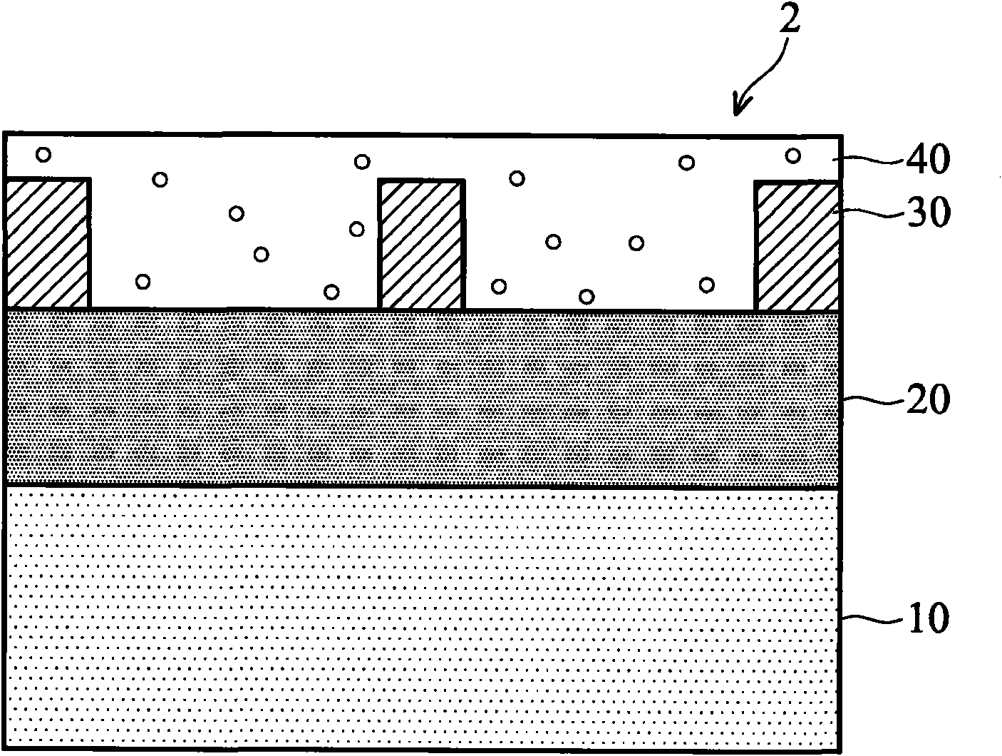
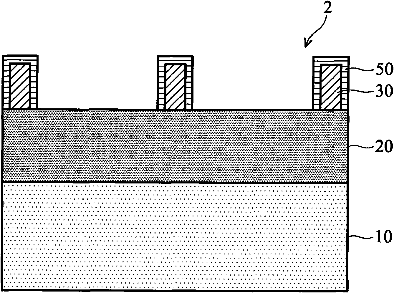
[0016] The present invention discloses a dual patterning method, which uses water-soluble polymer materials or water-soluble crosslinkable materials to replace traditional alcohol-based materials to produce resist patterns with overall enhanced etching resistance, which can be used to form submicron Fine-grained graphics required for semiconductor devices. according to Figure 1-Figure 8 A photolithography patterning method is shown, illustrating an embodiment of the device 2 at each stage of the process.
[0017] figure 1 A semiconductor device 2 having a silicon substrate 10 is shown. The substrate 10 may also be made of other suitable semiconductor materials, such as Ge, SiGe, or GaAs. Furthermore, the substrate 10 may be composed of other suitable elemental semiconductors, such as diamond; or be composed of a suitable compound semiconductor, such as silicon carbide, indium arsenide, or indium phosphide; or be composed of a suitable alloy semiconductor, such as silicon carbid...
PUM
 Abstract
Description
Claims
Application Information
 - R&D
- Intellectual Property
- Life Sciences
- Materials
- Tech Scout
- Unparalleled Data Quality
- Higher Quality Content
- 60% Fewer Hallucinations
Browse by: Latest US Patents, China's latest patents, Technical Efficacy Thesaurus, Application Domain, Technology Topic, Popular Technical Reports.
© 2025 PatSnap. All rights reserved.Legal|Privacy policy|Modern Slavery Act Transparency Statement|Sitemap|About US| Contact US: help@patsnap.com