
Manufacturing method of low-voltage transient voltage suppression diode chip

A technology of transient voltage suppression and manufacturing method, which is applied in semiconductor/solid-state device manufacturing, circuits, electrical components, etc., can solve problems such as increasing costs, and achieve the effect of increasing P/N junction depth and reducing surface leakage current.

Active Publication Date: 2010-01-06
BESTBRIGHT ELECTRONICS
View PDF3 Cites 16 Cited by
  • Summary
  • Abstract
  • Description
  • Claims
  • Application Information

AI Technical Summary

Problems solved by technology

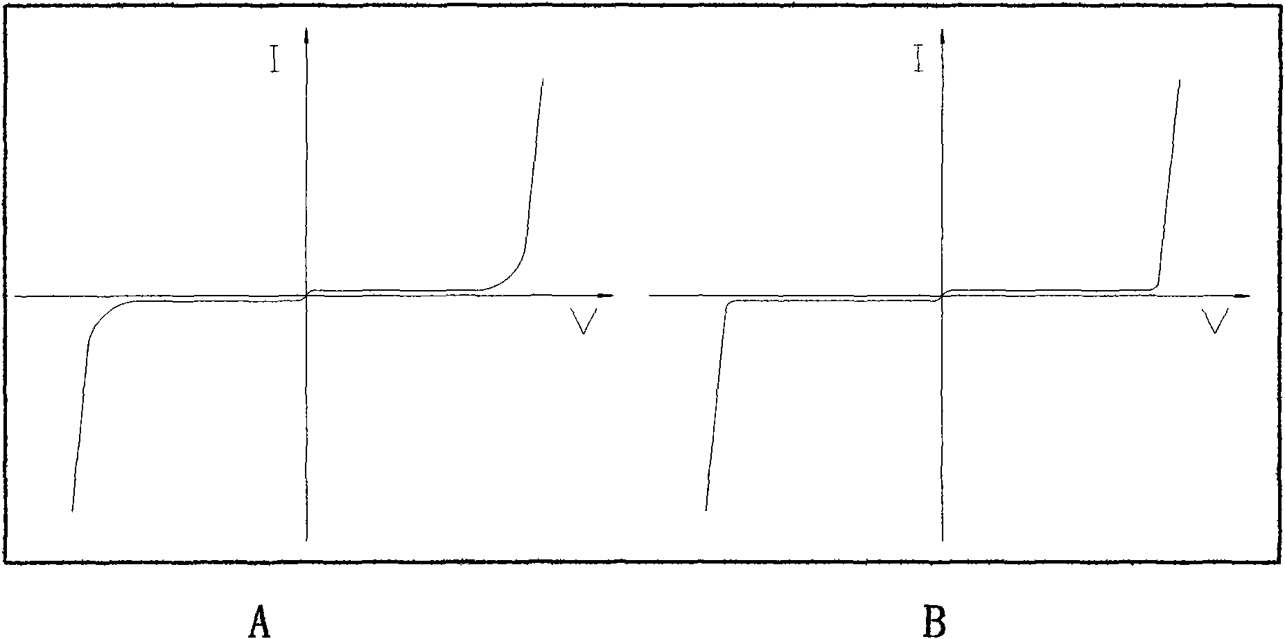
In order to make a bidirectional transient voltage suppressor, a circuit has been proposed in which two transient voltage suppressors are antiparallel. This solution requires more than one device to obtain the intended function and increases the cost.

Method used


Image

  • Manufacturing method of low-voltage transient voltage suppression diode chip
  • Manufacturing method of low-voltage transient voltage suppression diode chip

Examples


Embodiment Construction

[0023] The manufacturing method of the low-voltage transient voltage suppression diode chip of the invention will be further described in detail below in conjunction with the accompanying drawings.

[0024] Such as figure 1 and figure 2 As shown, the present invention uses a single-crystal silicon grinding disc with a resistivity of 0.001-0.02 Ω·cm in the P-type crystal orientation, and first performs chemical polishing treatment to remove the surface defect layer of the ground silicon wafer. Use nitric acid, hydrofluoric acid, and glacial acetic acid mixed acid according to the ratio of polishing to carry out polishing treatment on the silicon wafer at low temperature, and the thickness of single-side etching is 5-30um.

[0025] The polished silicon wafers are heat treated with a high-low-high temperature curve. First, perform one-step high-temperature annealing, and then continue the multi-step temperature-increasing heat treatment process at 750-900°C. Annealing is carr...


PUM

PropertyMeasurementUnit
electrical resistivityaaaaaaaaaa

Abstract

The invention discloses a manufacturing method of a low-voltage transient voltage suppression diode chip, which is characterized by comprising the following steps: a. selecting a P type crystal orientation monocrystalline silicon piece with resistivity of 0.001-0.02 omega*cm; carrying out chemical polishing and heat treatment gettering technologies on the monocrystalline silicon piece to reduce the defects and the impurity concentration of the surface and near a P / N nodal area of the monocrystalline silicon piece so as to realize the characteristic of low internal current leakage; c. doping chlorine, thermally oxidizing and passivating a P / N nodal surface; and d. bending a P / N node on the edge part of the P / N nodal surface towards a P area through a thermal oxidation technology so as to realize the characteristic of low surface current leakage. The invention can effectively reduce the reverse current leakage.

Description

technical field [0001] The invention relates to a manufacturing process of a semiconductor diode chip, in particular to a manufacturing method of a low-voltage transient voltage suppression diode chip. Background technique [0002] Transient suppression diode (TVS), also known as clamping diode, is a high-efficiency circuit protection device commonly used in the world. Its shape is the same as that of ordinary diodes, but it can absorb surge power up to several thousand watts. Its characteristic is that under reverse application conditions, when it is subjected to a high-energy large pulse, its working impedance immediately drops to an extremely low conduction value, thereby allowing a large current to pass, and at the same time controlling the voltage at a predetermined level, so it can Effective protection of precision components in electronic circuits. It can be used for lightning protection, overvoltage prevention, anti-interference, surge power absorption, etc. It is a...

Claims


Application Information

Patent Timeline
Patent Type & Authority Applications(China)
IPC IPC(8): H01L21/329H01L21/324
Inventor 曾国修李建利黄亚发
Owner BESTBRIGHT ELECTRONICS
Learn More