


Quick Research
Generate reliable direction feasibility study reports for your R&D in just a few steps.

Technical Q&A
Discover and master advanced knowledge NOW. Basics, ideas, possibilities, all at once.

Find Solutions
As an expert in R&D theories, this can generate solutions to your technical problems instantly.

Evaluate Feasibility
Analyze your overall solution with one click, know your potential R&D risks in advance.

Monitor Landscape
Get weekly tech updates, stay abreast of the latest tech innovations and key insights.
LED with coarsing interface and manufacturing method thereof
A technology of light-emitting diodes and manufacturing methods, which is applied in the direction of electrical components, circuits, semiconductor devices, etc., and can solve problems such as application limitations, uneven distribution of roughened surfaces, and inability to effectively improve external quantum efficiency.
- Summary
- Abstract
- Description
- Claims
- Application Information
AI Technical Summary
Problems solved by technology
Method used
Image

Examples
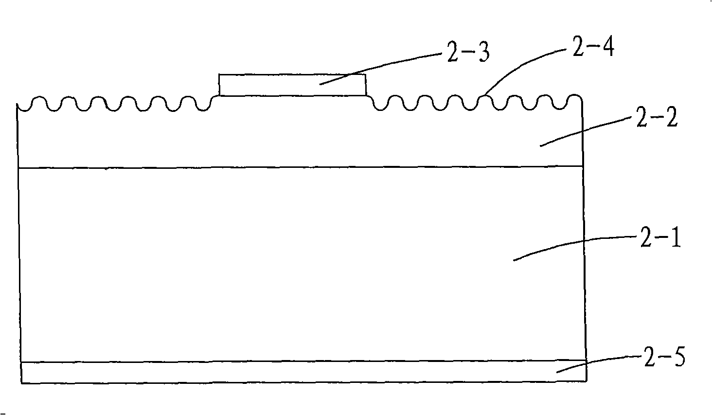
Embodiment 1
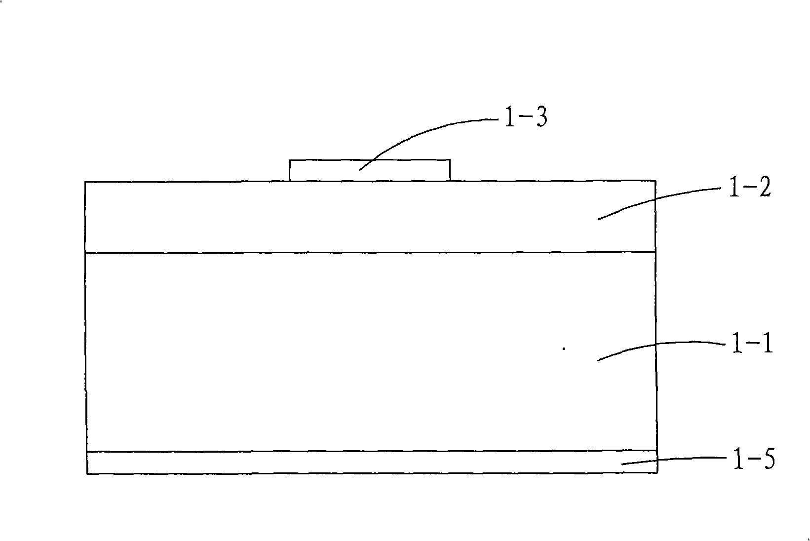
[0034] First provide a substrate 2-1;
[0035] Then use known techniques, such as metalorganic chemical vapor epitaxy (MOCVD), molecular beam epitaxy (MBE), etc. to grow into a light-emitting structure 2-2;
[0036] The first electrode 2-3 is formed on the light-emitting structure 2-2 by means of vapor deposition or sputtering (known technology) to plate gold beryllium and nickel.
[0037] Then use a rapid heat treatment method to fuse the first electrode 2-3 and the light-emitting structure 2-2 at high temperature, the heat treatment temperature is 400-800°C, and the time is 1-2 minutes;
[0038] The fused wafer is subjected to exposure, development, and etching processes (known technology), and the etching is wet etching, and the etching solution includes: one or more of chemical preparations such as iodine, potassium iodide, nitric acid, hydrochloric acid, sulfuric acid, and hydrofluoric acid Composition, etch out the light-emitting region, and then obtain the roughened in...
Embodiment 2
[0041] First, a substrate 2-1 is provided.
[0042] Then, the light-emitting structure 2-2 is grown by using known techniques, such as metalorganic chemical vapor epitaxy (MOCVD), molecular beam epitaxy (MBE), and the like.
[0043] Gold beryllium and nickel are plated by evaporation or sputtering to form the first electrode 2-3 on the light emitting structure 2-2.
[0044] Then, the first electrode 2-3 and the light-emitting structure 2-2 are fused at high temperature by conventional heat treatment. The heat treatment temperature is 400-800°C, and the time is 15-20 minutes.
[0045] The fused wafer is subjected to exposure, development, and etching processes, and the etching is wet etching. The etching solution contains: one or more of chemical agents such as iodine, potassium iodide, nitric acid, hydrochloric acid, sulfuric acid, and hydrofluoric acid. The light-emitting area, and then the roughened interface 2-4 is obtained.
Embodiment 3
[0048] First, a substrate 2-1 is provided.
[0049] Then, the light-emitting structure 2-2 is grown by using known techniques, such as metalorganic chemical vapor epitaxy (MOCVD), molecular beam epitaxy (MBE), and the like.
[0050] Gold beryllium is plated by evaporation or sputtering to form a first electrode 2-3 on the light emitting structure 2-2.
[0051] Then, the first electrode 2-3 is fused with the light emitting structure 2-2 at high temperature by means of rapid heat treatment. The heat treatment temperature is 400-800°C, and the time is 1-2 minutes.
[0052] The fused wafer is subjected to exposure, development, and etching processes, and the etching is wet etching. The etching solution contains: one or more of chemical agents such as iodine, potassium iodide, nitric acid, hydrochloric acid, sulfuric acid, and hydrofluoric acid. The light-emitting area, and then the roughened interface 2-4 is obtained.
[0053] Finally, gold germanium and nickel are plated on th...
PUM
 Abstract
Description
Claims
Application Information
 - R&D Engineer
- R&D Manager
- IP Professional
- Industry Leading Data Capabilities
- Powerful AI technology
- Patent DNA Extraction
Browse by: Latest US Patents, China's latest patents, Technical Efficacy Thesaurus, Application Domain, Technology Topic, Popular Technical Reports.
© 2024 PatSnap. All rights reserved.Legal|Privacy policy|Modern Slavery Act Transparency Statement|Sitemap|About US| Contact US: help@patsnap.com