ZnO base luminescent part with adulteration layer structure
A zinc oxide-based, light-emitting device technology, applied to laser parts, lasers, semiconductor devices, etc., to achieve the effect of simple process and easy formation
- Summary
- Abstract
- Description
- Claims
- Application Information
AI Technical Summary
Problems solved by technology
Method used
Image

Examples
Embodiment 1
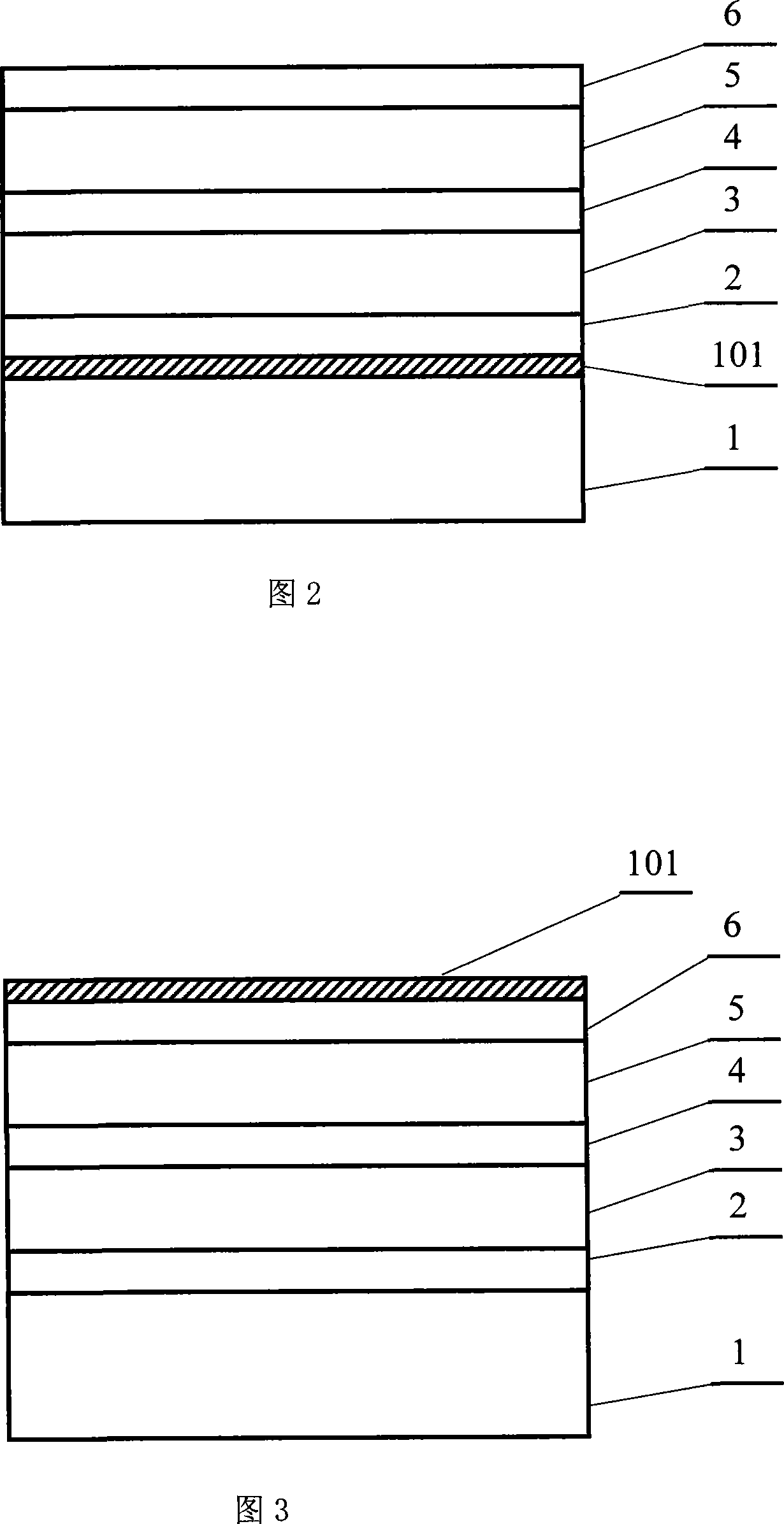
[0017] Down-doped interlayer ZnO-based light-emitting devices. The chip material structure of the down-doped interlayer type ZnO-based light-emitting device is shown in FIG. Its preparation process is, with Al 2 o 3 Substrate is taken as an example, substrate 1 is chemically cleaned, and the steps are: ultrasonic cleaning with toluene for 5 minutes, ultrasonic cleaning with acetone for 5 minutes, ultrasonic cleaning with ethanol for 5 minutes, and then recirculation once, and then rinsed with deionized water, and the substrate Put the bottom into H at a constant temperature of 160°C 2 SO 4 : HPO 3 = 3:1 (volume ratio) mixed solution for 10 minutes, and finally washed with deionized water, dried with high-purity nitrogen, and then used. Deposit a thin layer of doped interlayer 101 on the processed substrate, with a layer thickness of about 50 nanometers. The deposition method is here to use the sputtering method as an example. We use the SP-4 multifunctional magnetron deve...
Embodiment 2
[0019] Top-doped interlayer ZnO-based light-emitting devices. The chip material structure of the top-doped interlayer type ZnO-based light-emitting device is shown in FIG. The growth and treatment of the corresponding layers in the preparation process are the same as in Example 1. Control the temperature and time of annealing, so that the dopant element diffused into the doped interlayer 101 on the ZnO-based material upper confinement layer 5 and ZnO-based material cap layer 6 is transformed into p-type; the advantage of this device structure is that the doped interlayer 101 It is deposited last and will not affect the growth quality of the previous ZnO-based material. At the same time, the thickness of the doped interlayer 101 can be appropriately thicker, up to about 150 nanometers.
Embodiment 3
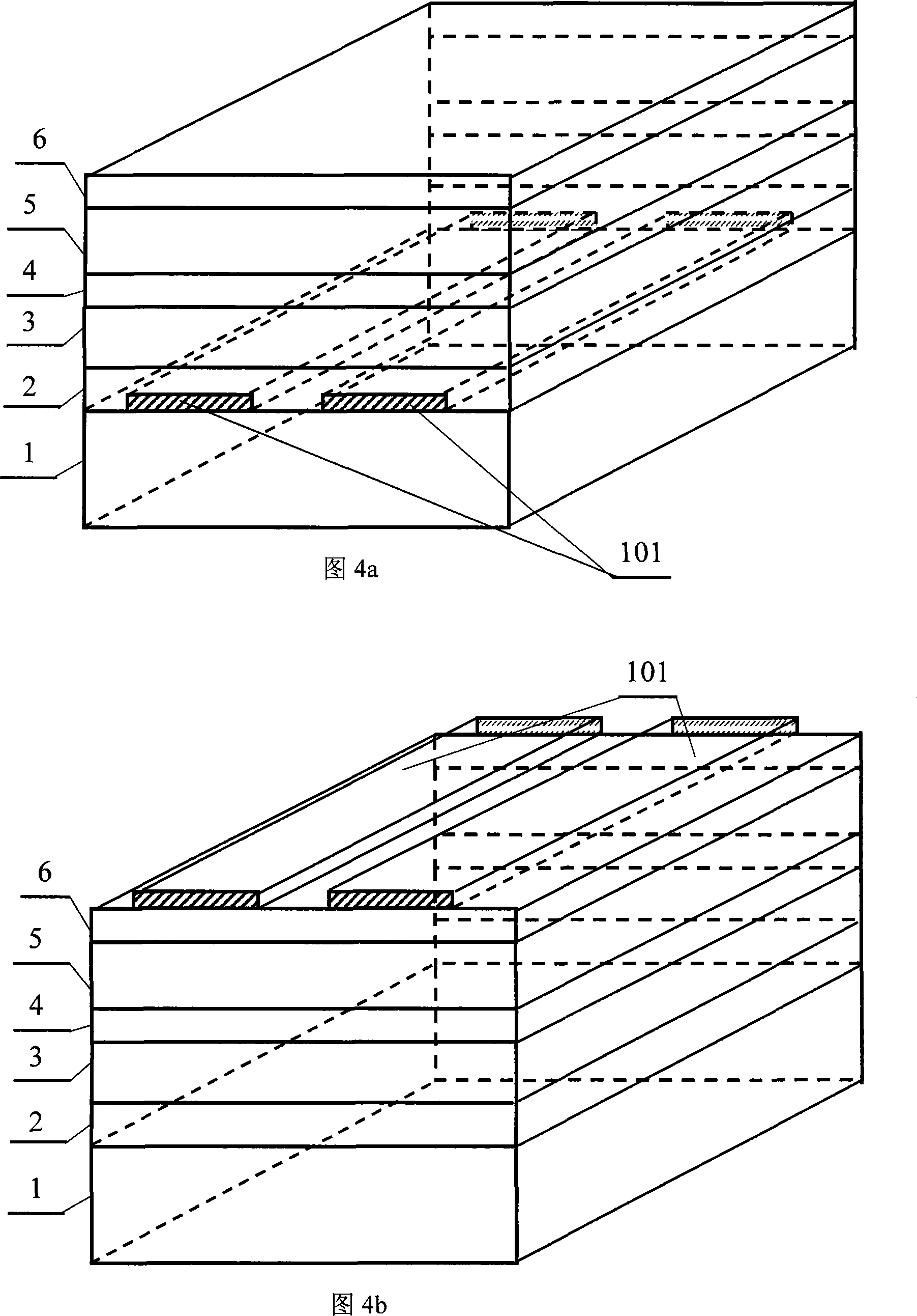
[0021] Pattern-doped interlayer ZnO-based light-emitting device. The chip material structure of this pattern-doped interlayer type ZnO-based light-emitting device is shown in Figure 4. The figure given in the figure is a double-stripe shape, which is formed on a cleaned substrate by using a conventional photolithography process. After the pattern of the plastic mask, after the GaAs layer is covered by the conventional sputtering method, the mask photoresist is further removed, or the mask method is used to make the corresponding pattern mask and place it on the continuously grown epitaxial wafer. The doped interlayer 101 is deposited by methods such as sputtering. The chip material structure of this doped interlayer type ZnO-based light-emitting device can be the lower-doped interlayer-type ZnO-based light-emitting device of Embodiment 1, which can be called the lower-pattern doped interlayer-type ZnO-based light-emitting device; it can also be the one of Embodiment 2. The to...
PUM
| Property | Measurement | Unit |
|---|---|---|
| thickness | aaaaa | aaaaa |
| thickness | aaaaa | aaaaa |
Abstract
Description
Claims
Application Information
 - R&D
- Intellectual Property
- Life Sciences
- Materials
- Tech Scout
- Unparalleled Data Quality
- Higher Quality Content
- 60% Fewer Hallucinations
Browse by: Latest US Patents, China's latest patents, Technical Efficacy Thesaurus, Application Domain, Technology Topic, Popular Technical Reports.
© 2025 PatSnap. All rights reserved.Legal|Privacy policy|Modern Slavery Act Transparency Statement|Sitemap|About US| Contact US: help@patsnap.com