Soldering method, component to be joined by the soldering method, and joining structure

a technology of soldering and components, applied in the direction of solventing apparatus, manufacturing tools, transportation and packaging, etc., can solve the problems of phase separation, the effect of thermal fatigue resistance, the effect of preventing the deterioration of the soldering portion and sufficient strength of thermal fatigue resistan

Inactive Publication Date: 2009-01-06
PANASONIC CORP
View PDF14 Cites 4 Cited by
  • Summary
  • Abstract
  • Description
  • Claims
  • Application Information

AI Technical Summary

Benefits of technology

[0022]The object of the invention is to provide a soldering method that can prevent deterioration of the soldering portion (or joining portion) caused by continuous use under a condition of high temperature and can obtain a sufficient strength of thermal fatigue resistanc

Problems solved by technology

Although other components than the soldering material such as the flux can exist in the joining portion, these other components causes phase separation from the soldering material at the thermal treatment, fail to exist inside the joining portion, and only remain slightly on the surface of the portion.
In recent years, the waste disposal of electronic equipment having the above-described electronic circuit board have offered a problem, and effects on the global environment and the human body exerted by the lead (Pb) contained in soldering materials have become a matter of concern.
Although use of the Sn—Zn series materials in place of the Sn—Pb series materials had an advantage of soldering

Method used


Image

  • Soldering method, component to be joined by the soldering method, and joining structure
  • Soldering method, component to be joined by the soldering method, and joining structure

Examples


Embodiment Construction

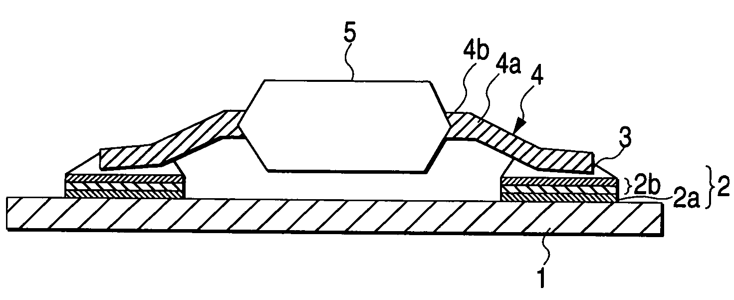
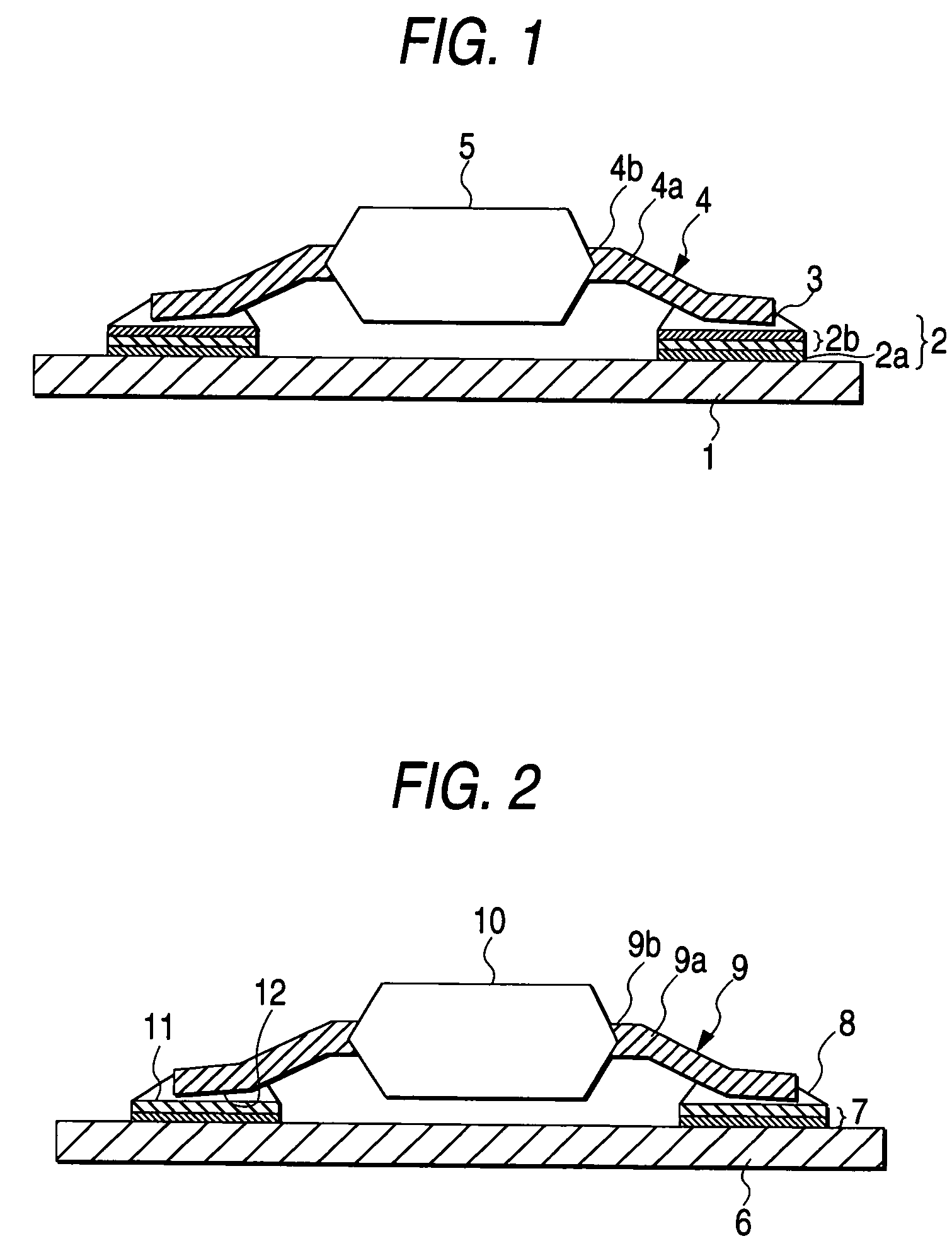
[0043]One mode for execution is hereinafter illustrated through FIG. 1. FIG. 1 is a schematic partial sectional view of an electronic circuit board prepared by the soldering method in this mode for execution.

[0044]First, a board 1 and electronic component 5 to be joined thereto are prepared. A land 2 prepared by covering a parent material 2a comprising Cu with a barrier metal layer 2b comprising a Ni layer and an Au layer is formed on the board 1, and the land 2 can be formed, for example, according to the following method.

[0045]For example, the parent material 2a comprising Cu is formed in one united body with a wiring pattern (not shown in the figure) on the upper surface of the board 1 made of a glass epoxy resin or the like by thermo-compression bonding (or mounting) of copper foil and etching. The wiring pattern can have a width of, for example, about 50 to about 100 μm. Thereafter, a resist is formed in a prescribed region of the surface of the board 1 to cover the wiring patt...


PUM

PropertyMeasurementUnit
Thicknessaaaaaaaaaa

Abstract

It is possible to prevent deterioration of a soldering portion and improve strength of thermal fatigue resistance by providing barrier metal layers on at least one of lead and land to cover parent materials comprising Cu-containing materials, feeding a soldering material between the lead and the land and allowing to contact in a fused condition with barrier metal layers and solidify, and thus soldering together the lead and the land.

Description

[0001]The present application is based on Japanese Patent Application No. 2003-028032, which is incorporated herein by reference.BACKGROUND OF THE INVENTION[0002]1. Field of the Invention[0003]The present invention relates to a method for soldering one member to another member, and more specifically to a method for soldering a land formed on a board and an electrode of electronic component (e.g., lead) in a process of manufacturing an electronic circuit board. Furthermore, the invention relates to a joining structure obtained by this soldering method and an electrical component or an electronic component used in this soldering method.[0004]2. Description of the Related Art[0005]In processes for manufacturing an electronic circuit board used for the electronic equipment, the method of reflow soldering has hitherto been known as one of methods used for mounting an electronic component on a board, more specifically for joining electrically and physically a lead pulled out of the electr...

Claims


Application Information

Patent Timeline
IPC IPC(8): B32B15/01B23K20/16B23K35/00B23K35/26H01L23/488H01L23/498H01L23/50H05K3/24H05K3/34
CPCB23K20/16H01L23/488H01L23/49811H05K3/3463B23K35/007Y10T428/12882B23K35/262B23K2201/40H05K3/244H05K3/3426H01L2924/0002Y10T428/12708Y10T428/12792H01L2924/00B23K2101/40
Inventor YAMAGUCHI, ATSUSHINISHIDA, KAZUTOHIRANO, MASATO
Owner PANASONIC CORP
Why Eureka
Try Eureka