Semiconductor integrated circuit device and a method of manufacturing the same

Inactive Publication Date: 2006-04-04
HITACHI LTD
View PDF12 Cites 2 Cited by
  • Summary
  • Abstract
  • Description
  • Claims
  • Application Information

AI Technical Summary

Benefits of technology

[0007]With recent high integration and scale-down of a semiconductor integrated circuit in particular, there is a tendency to reduce the area of each memory cell. As a result, information storage units, i.e., a pair of drive n channel type MISFETs and a pair of load p channel type MISFETs are reduced in distance therebetween and susceptible to an α ray. There is a tendency to reduce a source voltage (Vcc) for the purpose of a reduction in power consumption. Thus, the rate of occurrence of the soft error due to the α ray rises.
[0012]An object of the present invention is to provide a semiconductor integrated circuit device, e.g., a high-performance semiconductor integrated circuit device which reduces a soft error produced in each memory cell of an SRAM.
[0013]Another object of the present invention is to improve the performance of a semiconductor integrated circuit device, e.g., a system LSI wherein an SRAM and a device having an analog capacitor are formed on a single substrate.

Problems solved by technology

With recent high integration and scale-down of a semiconductor integrated circuit in particular, there is a tendency to reduce the area of each memory cell.
However, a tunnel current occurs in such a capacitor with thinning of the gate insulating film.
As a result, a leak current increases.

Method used


Image

  • Semiconductor integrated circuit device and a method of manufacturing the same
  • Semiconductor integrated circuit device and a method of manufacturing the same
  • Semiconductor integrated circuit device and a method of manufacturing the same

Examples


first embodiment

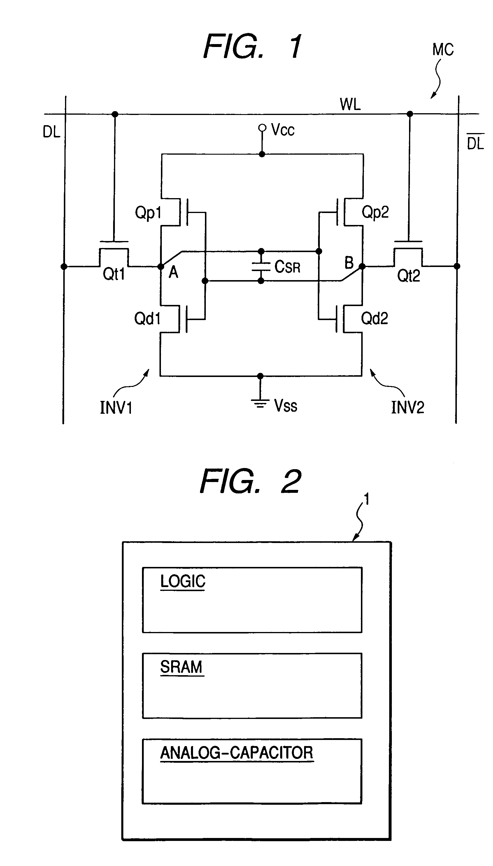
[0065]FIG. 1 is an equivalent circuit diagram showing a memory cell of a SRAM illustrative of the first embodiment. As shown in the drawing, the memory cell MC is placed in a portion where a pair of complementary data lines (a data line DL and a data line / (bar) DL) and a word line WL intersect, and comprises a pair of drive MISFETs Qd1 and Qd2, a pair of load MISFETs Qp1 and Qp2, and a pair of transfer MISFETs Qt1 an Qt2. The drive MISFETs Qd1 and Qd2 and the transfer MISFETs Qt1 and Qt2 respectively comprise n channel type MISFETs, whereas the load MISFETs Qp1 and Qp2 comprise p channel type MISFETs respectively.

[0066]In the six MISFETs constituting the memory cell MC, the drive MISFET Qd1 and the load MISFET Qp1 constitute a CMOS inverter INV1, and the drive MISFET Qd2 and the load MISFET Qp2 constitute a CMOS inverter INV2. Mutual input / output terminals (storage nodes A and B) of one pair of these CMOS inverters INV1 and INV2 are coupled to each other so as to intersect and cons...

second embodiment

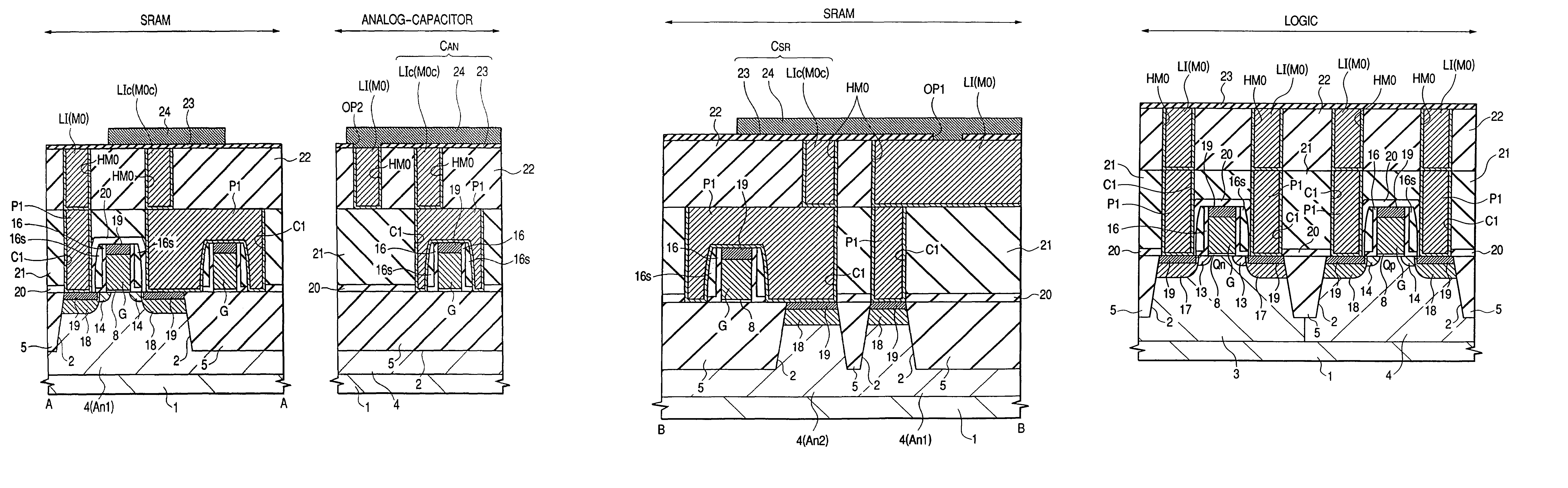
[0146]A semiconductor integrated circuit device according to the present embodiment will next be described in accordance with its manufacturing process. FIGS. 41 through 44 are respectively fragmentary cross-sectional views or plan views of a substrate, showing a method of manufacturing the semiconductor integrated circuit device according to the present embodiment. Incidentally, since the process steps up to the formation of the local Wirings L1 (M0) and LIc (M0c) described using FIGS. 2 through 26 are similar to the first embodiment, the description thereof will be omitted.

[0147]The semiconductor substrate 1 shown in FIGS. 23 through 26 described in the first embodiment is first prepared. The local wirings LI (M0) and LIc (M0c) shown in these drawings are formed by depositing the thin barrier layer formed of, for example, the TiN film over the silicon oxide film 22 including the interiors of the wiring trenches HM0 formed in the silicon oxide film 22 by the sputtering method, next...


PUM


Abstract

In order to improve the performance of a semiconductor integrated circuit device wherein a capacitor provided between storage nodes of an SRAM and a device having an analog capacitor are formed on a single substrate, a plug is formed in a silicon oxide film on a pair of n channel type MISFETs in a memory cell forming area, and a local wiring LIc for connecting respective gate electrodes and drains of the pair of n channel type MISFETs is formed over the silicon oxide film and the plug. Thereafter, a capacitive insulating film and an upper electrode are further formed over the local wiring LIc. According to the same process step as the local wiring, capacitive insulating film and upper electrode formed in the memory cell forming area, a local wiring LIc, a capacitive insulating film and an upper electrode are formed over a silicon oxide film in an analog capacitor forming area and a plug in the silicon oxide film.

Description

[0001]This application is a Continuation of nonprovisional U.S. application Ser. No. 10 / 308,001 filed Dec. 3, 2002. Priority is claimed based on U.S. application Ser. No. 10 / 308,001 filed Dec. 3, 2002 now U.S. Pat. No. 6,762,444, which claims the priority of Japanese Application No. 2001-183098 filed on Jun. 18, 2001.TECHNICAL FIELD[0002]The present invention relates to a semiconductor integrated circuit device and a technology for manufacturing the same, and particularly to a technology effective for application to a semiconductor integrated circuit device having an SRAM (Static Random Access Memory).BACKGROUND OF THE INVENTION[0003]An SRAM has been used as a cache memory used for a personal computer and a work station.[0004]The SRAM comprises a flip-flop circuit for storing one-bit information therein and two information transfer MISFETs (Metal Insulator Semiconductor Field Effect Transistors). The flip-flop circuit comprises, for example, a pair of drive MISFETs and a pair of loa...

Claims


Application Information

Patent Timeline
IPC IPC(8): H01L21/336H01L21/00H01L21/48H01L21/8234H01L21/768H01L21/822H01L21/8244H01L27/04H01L27/10H01L27/11
CPCH01L27/1104H01L27/11H10B10/00H10B10/12H10B99/00
Inventor OOTSUKA, FUMIONONAKA, YUSUKESHIMAMOTO, SATOSHIOMORI, SOHEIKAZAMA, HIDETO
Owner HITACHI LTD
Why Eureka
Try Eureka