
Casting method for producing surface acoustic wave devices

a surface acoustic wave and casting method technology, applied in the field of devices, can solve the problems of micro-cracks or variations on the surface of mechanical polishing, difficult and tedious mechanical grinding and polishing, and often exceed the cost of making the diamond film itsel

Inactive Publication Date: 2006-03-14
SUNG CHIEN MIN
View PDF31 Cites 12 Cited by
  • Summary
  • Abstract
  • Description
  • Claims
  • Application Information

AI Technical Summary

Benefits of technology

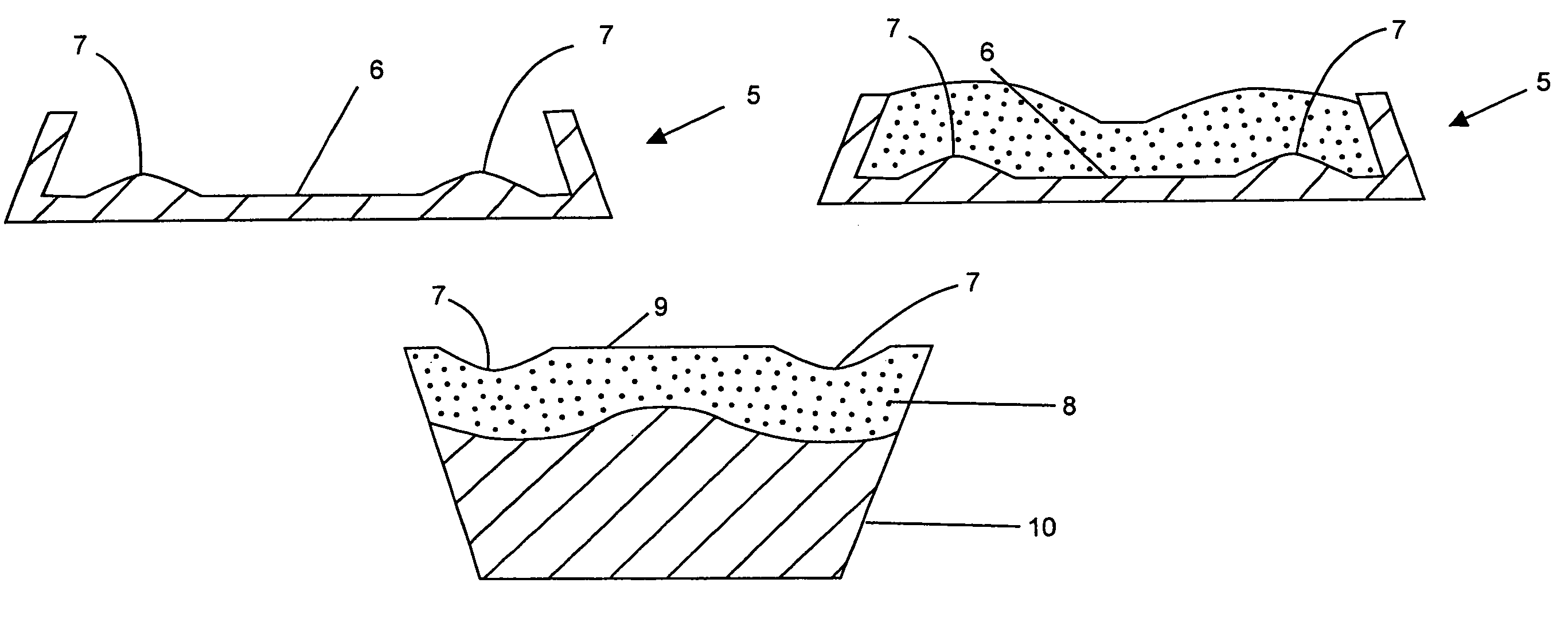
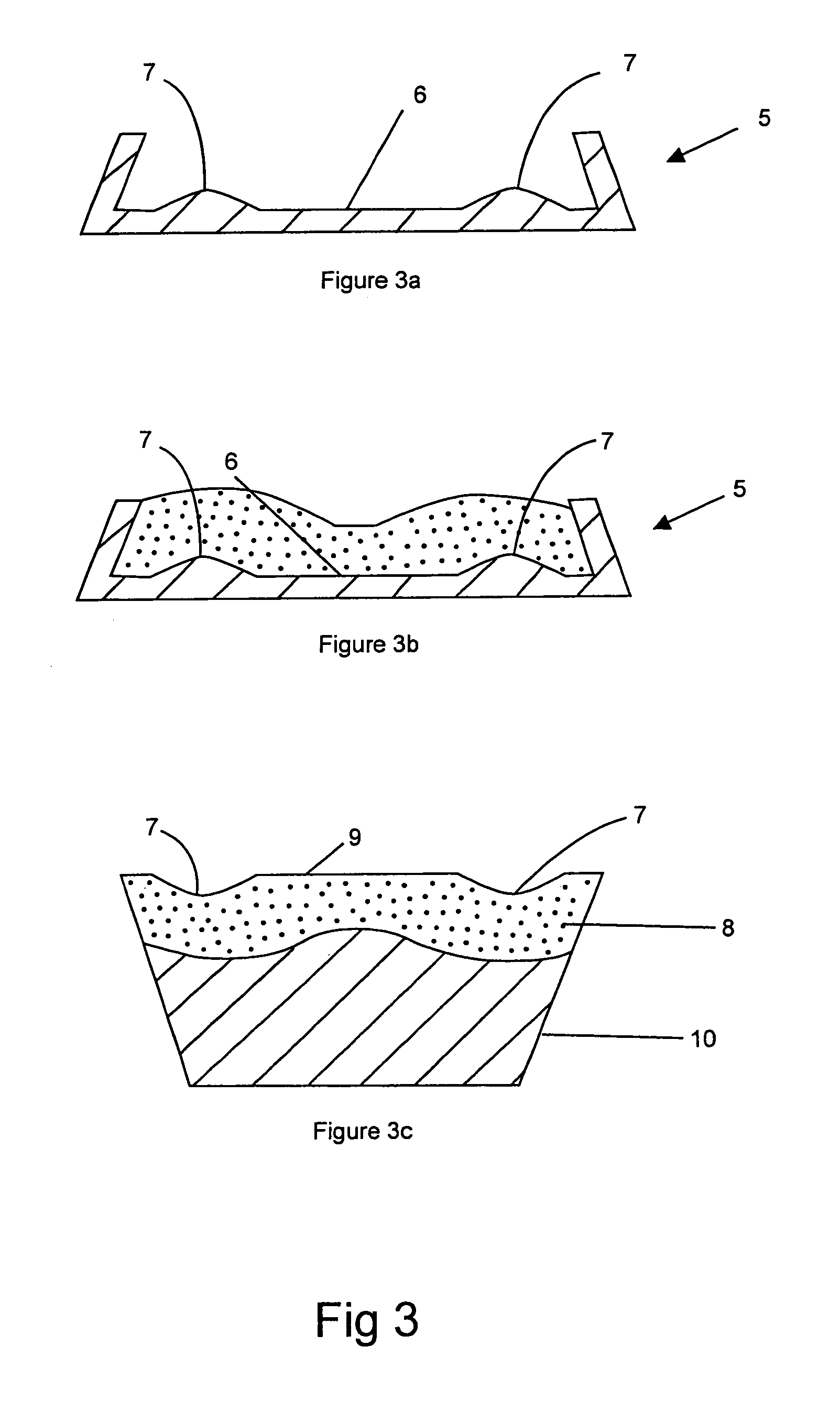
"The present invention provides diamond tools and methods for making them without requiring post-fabrication polishing or finishing of the working surface. These tools have a super-hard working surface with minimal micro-cracks and variations, making them ideal for use in SAW filters. The method involves growing an adynamic diamond layer on a mold, which is then joined to a support layer. A piezoelectric layer can be coupled to the working surface of the diamond using various techniques, such as forming the mold as a piezoelectric material or bonding a thin piezoelectric layer to the working surface. The invention also allows for the simultaneous fabrication of multiple SAW filters by forming grooves in a mold and separating them after the adynamic diamond layer and support material are formed."

Problems solved by technology

However, as diamond and diamond-like substances are among the hardest known materials, such mechanical grinding and polishing is difficult and tedious.
Moreover, the cost of polishing often exceeds the cost for making the diamond film itself.
In addition, mechanical polishing inevitably introduces micro-cracks or variations on the diamond surface.
Such cracks and variations are detrimental to certain applications.
For example, if the diamond is used make a surface acoustic wave (SAW) filter, micro-cracks or variations in the diamond surface will introduce noise into the signal and therefore deteriorate the quality of the filtered wave.
However, these methods introduce surface defects which adversely effect performance.
As commercial pressures drive applications to use higher frequencies in order to accommodate greater amounts of information, the surface roughness will be a significant limiting factor.

Method used


Image

  • Casting method for producing surface acoustic wave devices
  • Casting method for producing surface acoustic wave devices
  • Casting method for producing surface acoustic wave devices

Examples


example 1

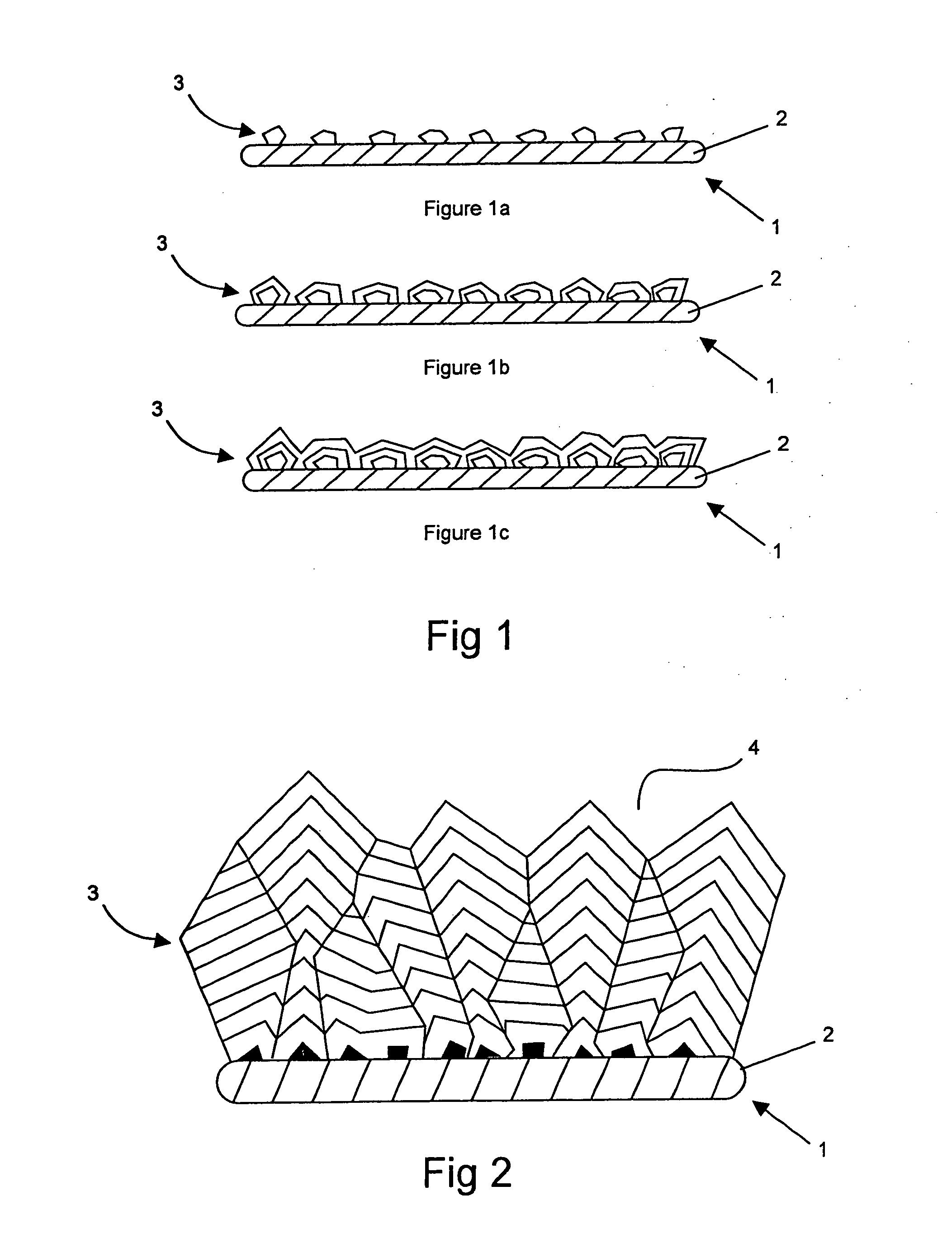
[0159]One side of a 0.7 mm thick silicon wafer is polished to a surface roughness of about 3 angstroms. The polished wafer is then placed in a CVD reactor using tungsten filaments and filled with hydrogen gas containing 1% by volume methane at 40 torr. The silicon wafer is maintained at a temperature of about 900° C. The process maintained for 10 hours, wherein the diamond layer thickness is about 10 micrometers. The silicon wafer is removed from the reactor, whereupon it is noted that the growth surface contains crystalline facets of several microns.

[0160]The growth surface of the diamond layer is then brazed to a tungsten support layer having a thickness of 2 mm using a braze foil. The braze foil is an amorphous nickel alloy (available under the tradename MBF-20 from Honeywell). The braze foil is placed between the growth surface of the diamond layer and the support layer and heated to 1010° C. under vacuum for 17 minutes. Upon cooling, a majority of the silicon is removed using a...

example 2

[0161]The same process as in Example 1, except the mold and support layers were titanium and the braze alloy was Ag—Cu—Ti alloy. A one micron thick layer of ZnO was deposited by sputtering on the working surface of the diamond under vacuum. Next, a one micron thick layer of aluminum was deposited on the ZnO. A portion of the aluminum layer was then etched away to form IDT pads to create a SAW filter. The resulting SAW filter performed well at frequencies above about 2 GHz.

example 3

[0162]Copper plates were polished to an Ra of about 5 nm using an ultrasonic bath of nano-sized diamond particles. After drying, the plates were placed in a CVD reactor and a diamond film of about 10 microns were deposited as described in Example 1. As the copper cools the thin diamond layer peels from the copper mold. A braze foil of 0.001 inches thick (MBF-20 as in Example 1) is placed on a tungsten support layer. The thin diamond layer is then pressed against the braze foil using a stainless steel block sprayed with boron nitride powder to form an assembly. The assembly is then heated to 1010° C. for about 8 minutes under vacuum of 10−5 torr.


PUM

PropertyMeasurementUnit
thicknessaaaaaaaaaa
thicknessaaaaaaaaaa
thicknessaaaaaaaaaa

Abstract

A method for forming diamond tools using CVD techniques. In one aspect, a mold is provided which has an interface surface configured to inversely match a configuration intended for the working surface of a diamond layer in a tool. An adynamic diamond mass or layer is then deposited upon the diamond interface surface of the mold, and a support layer is joined to the growth surface of the adynamic diamond layer. At least a portion of the mold is then removed to expose the working surface of the diamond which has received a shape which inversely corresponds to the configuration of the mold's diamond interface surface.

Description

PRIORITY DATA[0001]This application is a continuation-in-part of U.S. patent application Ser. No. 10 / 002,395, filed on Oct. 19, 2001, now U.S. Pat. No. 6,814,130 which is a continuation-in-part of U.S. patent application Ser. No. 09 / 687,444, filed on Oct. 13, 2000, now U.S. Pat. No. 6,659,161 both of which are incorporated herein by reference in their entireties.FIELD OF THE INVENTION[0002]The present invention relates to devices incorporating super-hard materials, such as diamond or diamond-like substances, and methods for making such devices. More particularly, the present invention relates to the use of chemical vapor deposition for making devices incorporating very thin layers of super-hard materials.BACKGROUND OF THE INVENTION[0003]Diamond and diamond-like substances have many properties, such as wear resistance, thermal conductivity, acoustic transmission, and corrosion inertness, which make them desirable for a variety of industrial applications. To this end, diamond and diam...

Claims


Application Information

Patent Timeline
Patent Type & Authority Patents(United States)
IPC IPC(8): B22D27/00C23C16/27C23C16/01C23C16/26H03H3/08
CPCC23C16/01C23C16/27C30B25/02H03H3/08H04R7/125C30B29/04H04R2307/027H04R2307/023
Inventor SUNG, CHIEN-MIN
Owner SUNG CHIEN MIN
Learn More