
Method for synthesizing n-type diamond having low resistance

Inactive Publication Date: 2002-01-22
JAPAN SCI & TECH CORP
View PDF9 Cites 35 Cited by
  • Summary
  • Abstract
  • Description
  • Claims
  • Application Information

AI Technical Summary

Benefits of technology

A p-type diamond thin film having low resistance can be easily manufactured by a conventional technique. Although an n-type diamond having high resistance can be manufactured, it is difficult to manufacture an n-type diamond thin film having low resistance because it is impossible to activate at room temperature (300.degree. K) due to the self-compensation effect and the deep donor level (500 meV).
If an n-type diamond having low resistance can be synthesized as a single crystal diamond thin film, by combining it with a p-type diamond having low resistance, which is already realized by doping impurities, it is possible to manufacture a high power and high speed semiconductor device using a diamond operable at high temperature and an ultraviolet semiconductor laser diode made of diamond, which is essential for a high density recording and a vast information transmittance.
It is also possible to manufacture a transparent n-type single crystal protective film utilizing high hardness of a diamond, which is excellent in electric conductivity and thermal conductivity. Furthermore, by utilizing the negative electron affinity energy of a diamond, it is possible to manufacture a display having a large surface area made by highly efficient electron beam materials of an n-type diamond having low resistance.
To form an n-type diamond having low resistance means to delete the deep donor level due to N in a synthesized diamond and change the deep level to a shallow level, whereby an absorption of natural light (sun light) is prevented, to thereby extinguish the color caused by the deep level of the single N in the synthetic diamond. This is the same as in forming a transparent synthesized diamond by forming an n-type diamond having low resistance. In synthesizing a diamond by a high-temperature and high-pressure synthetic technique utilizing nickel catalyst or the like, it becomes possible to manufacture a transparent diamond valuable as a jewel.
The inventor has found the facts that, in order to solve the aforementioned problems, in forming a single crystal diamond thin film on a substrate by a vapor-phase growth method or a sputtering method, by simultaneously doping a p-type dopant and an n-type dopant, it becomes possible to stabilize an n-type dopant in a high densitys, lower an impurity level and greatly increase the number of carriers, to thereby synthesize a high quality single crystal diamond thin film having low resistance.
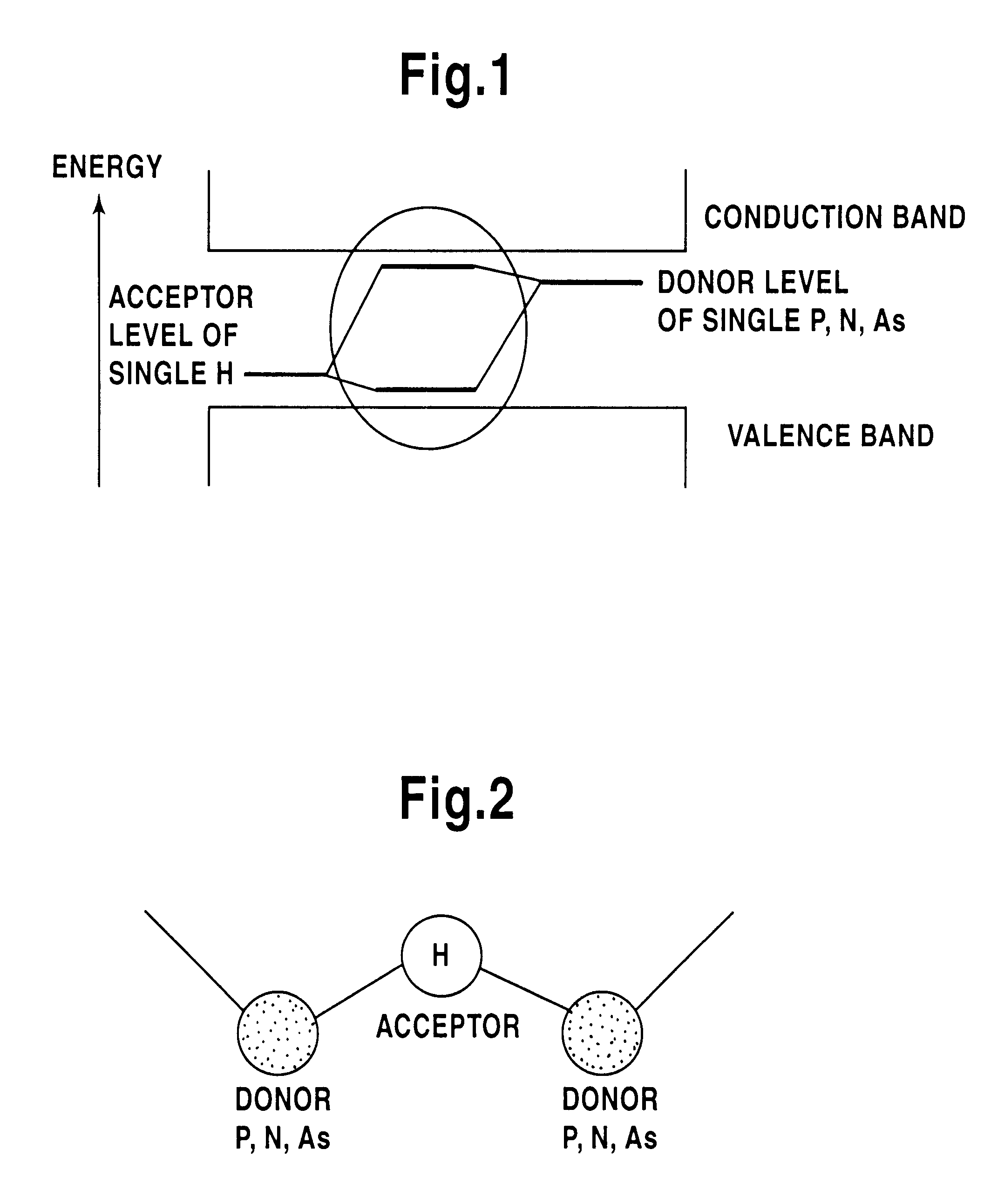
The inventor has also found the following fact. That is, in synthesizing an artificial diamond by a conventional high-temperature and high-pressure synthesizing method utilizing nickel catalyst or the like, by mixing H as a p-type dopant and N, P or As as an n-type dopant at the atomic density ratio of 1:2 to 1:3 before synthesizing, a donor-acceptor compound, such as a P--H--P pair, an N--H--N pair or a As--H--As pair, is formed in a crystal, to lower the impurity level as compared to a single doping to thereby form an n-type diamond having low resistance. This results in a transparent artificial diamond, wherein a conventional artificial diamond made by a conventional method had color because the natural light is absorbed by the deep impurity level of N.

Problems solved by technology

The above-mentioned plasma CVD method and thermal decomposing CVD method have drawbacks such that it is troublesome to execute the method due to the high-temperature processing, the obtained film is easily broken due to the residual stress maintained in the film, and it is difficult to control an amount of dopant.
Although an n-type diamond having high resistance can be manufactured, it is difficult to manufacture an n-type diamond thin film having low resistance because it is impossible to activate at room temperature (300.degree. K) due to the self-compensation effect and the deep donor level (500 meV).
Furthermore, by simultaneously doping an n-type dopant and a p-type dopant, a pair of an n-type dopant and a p-type dopant is formed in a diamond crystal, which decreases electron scattering of n-type carrier due to an n-type carrier dopant, to thereby increase the carrier movement, resulting in low resistance.

Method used


Image

  • Method for synthesizing n-type diamond having low resistance
  • Method for synthesizing n-type diamond having low resistance
  • Method for synthesizing n-type diamond having low resistance

Examples


examples

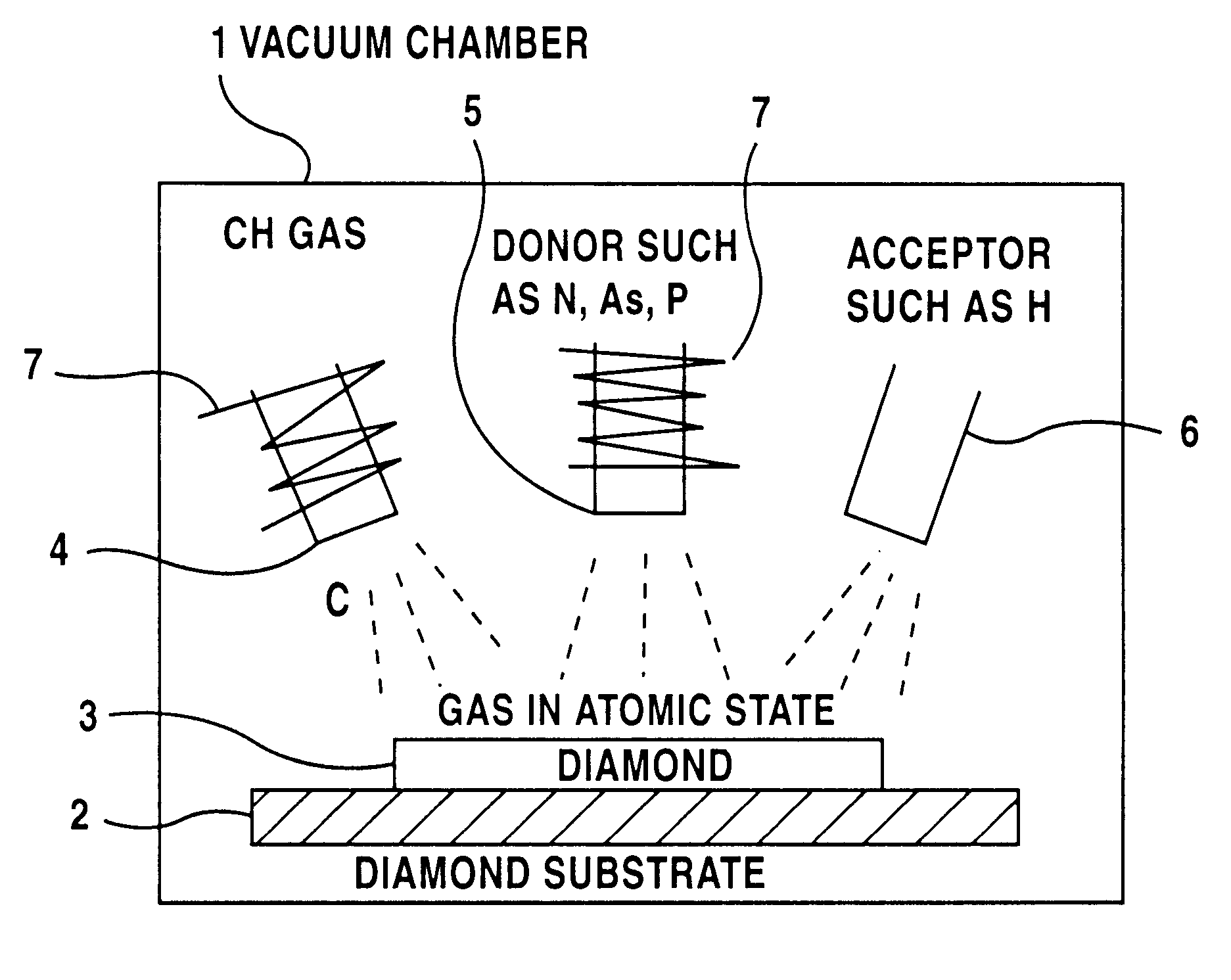
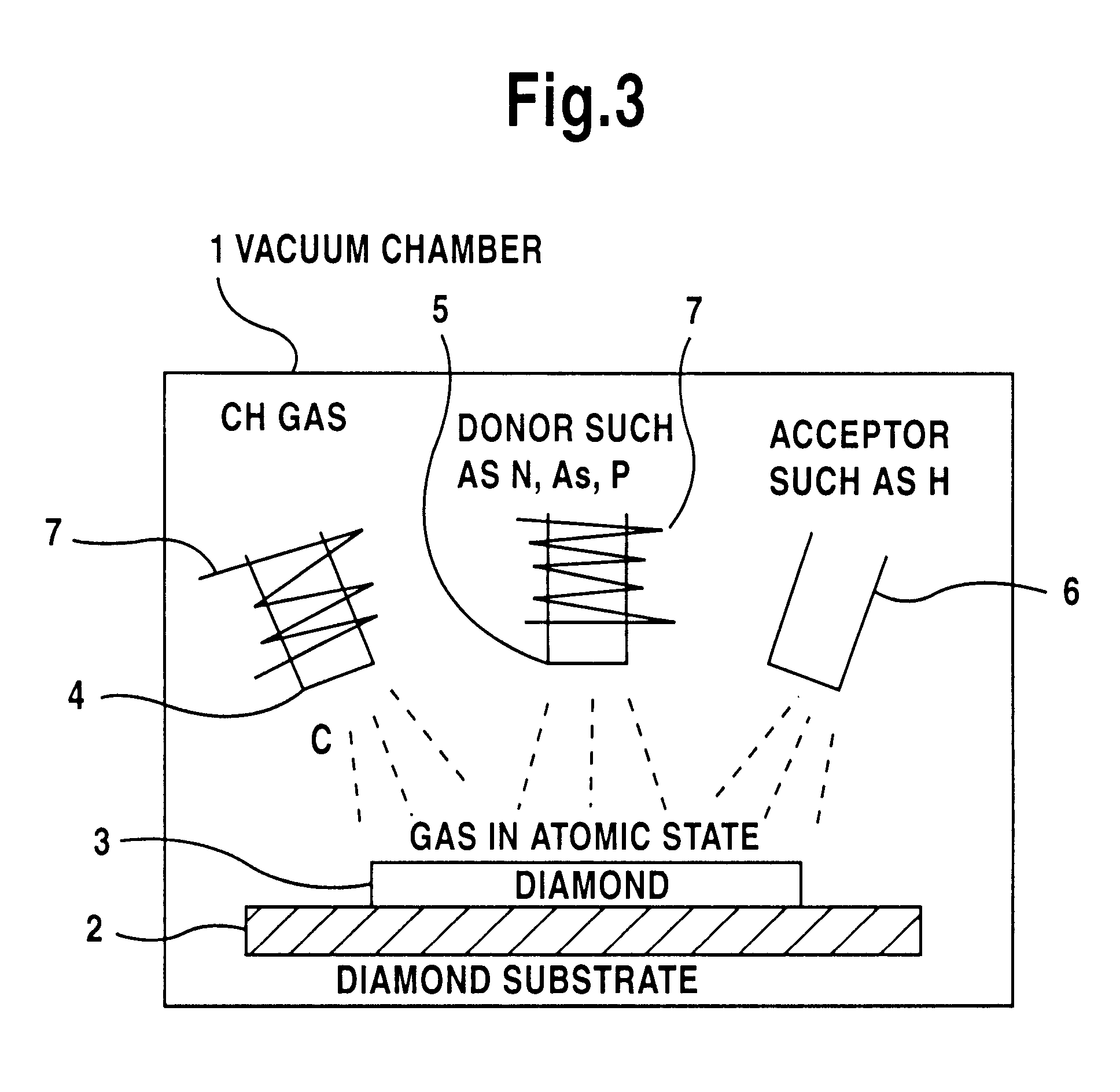
As shown in FIG. 3, the vacuum chamber 1 was maintained to be vacuum degree of 10.sup.-10 torr, and the substrate 2 was heated by the electrical heater. CH gas (hydrocarbon, methane, ethane, propane) was introduced through the gas introducing pipe 4, and was thermally decomposed by the RF coil 7 to supply the molecular flow toward the substrate 2 so as to be adsorbed on the substrate 2. P as a donor was emitted toward the substrate 2 through the introducing pipe 5 at the flow rate of 5.times.10.sup.-9 torr, and H as an acceptor was emitted toward the substrate 2 from the introducing pipe 6 at the flow rate of 10.sup.-9 torr so as to simultaneously dope them, to thereby form a diamond 3 at the substrate temperature of 400.degree. C., 450.degree. C., 600.degree. C., 800.degree. C. and 900.degree. C. P as a donor and H as an acceptor were electrically excited by the RF coil 7 so as to become an atomic gaseous state. After 90 minutes had passed, the crystal growth was interrupted.

The ob...


PUM

PropertyMeasurementUnit
Angleaaaaaaaaaa
Temperatureaaaaaaaaaa
Electrical resistanceaaaaaaaaaa

Abstract

In synthesizing a diamond by a vapor-phase growth method, a sputtering method, or a high-pressure and high-temperature synthesis method, N, P or As as an n-type dopant, and H as a p-type dopant are simultaneously doped in a crystal to form a donor-acceptor pair in the crystal, to thereby synthesize a transparent n-type diamond having low resistance.

Description

This invention relates to a method for synthesizing an artificial diamond, and more specifically, to a method for synthesizing a transparent n-type diamond having low resistance in manufacturing a diamond by a vapor-phase growth method, a sputtering method, a high-temperature and high-pressure synthesis method, or the like.TECHNICAL BACKGROUNDAs a method for synthesizing a diamond, a method for artificially synthesizing a diamond from a graphite carbon by using a catalyst under high-temperature and high-pressure (50 kbr, 1500 k or more), and a method for synthesizing a diamond thin film on a substrate by a CVD method from a mixed gas of a hydrocarbon and a hydrogen under low pressure (<1 Torr) and high temperature (>800.degree. C.), or the like, are known. Japanese Patent Unexamined Laid-open Publication No. S62(1987)-70295 discloses a method for manufacturing an n-type semiconductor diamond thin film. According to the method, a reaction gas comprising a gas including P, As or...

Claims


Application Information

Patent Timeline
IPC IPC(8): C23C14/06C23C16/26C30B25/02C23C16/27C30B23/02B01J3/06C30B29/04H01L21/203H01L21/205
CPCC23C14/0611C23C16/27C23C16/278C30B23/02C30B25/02C30B29/04
Inventor YOSHIDA, HIROSHI
Owner JAPAN SCI & TECH CORP
Learn More