Method of manufacturing a short-channel FET with Schottky-barrier source and drain contacts
- Summary
- Abstract
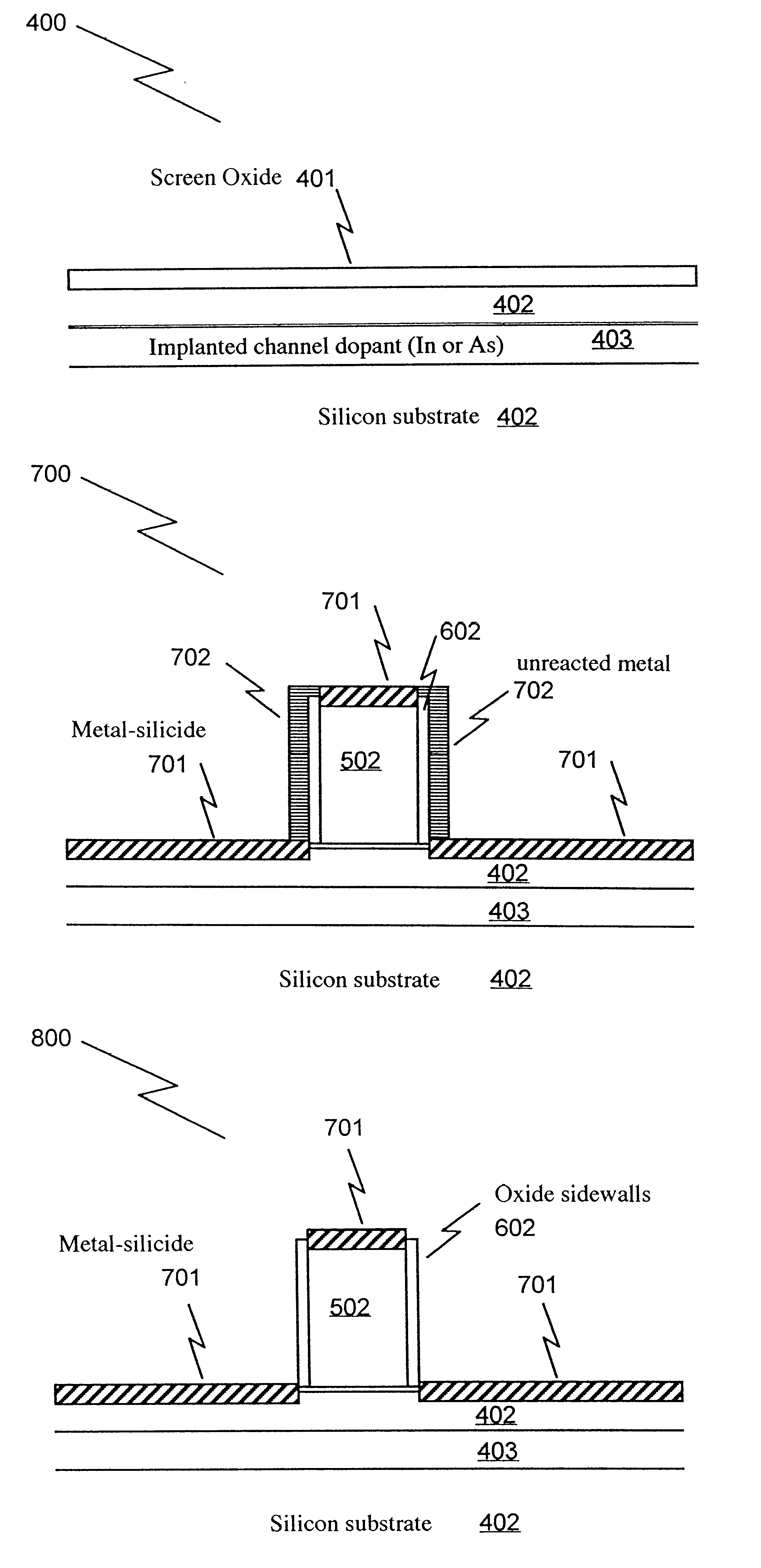
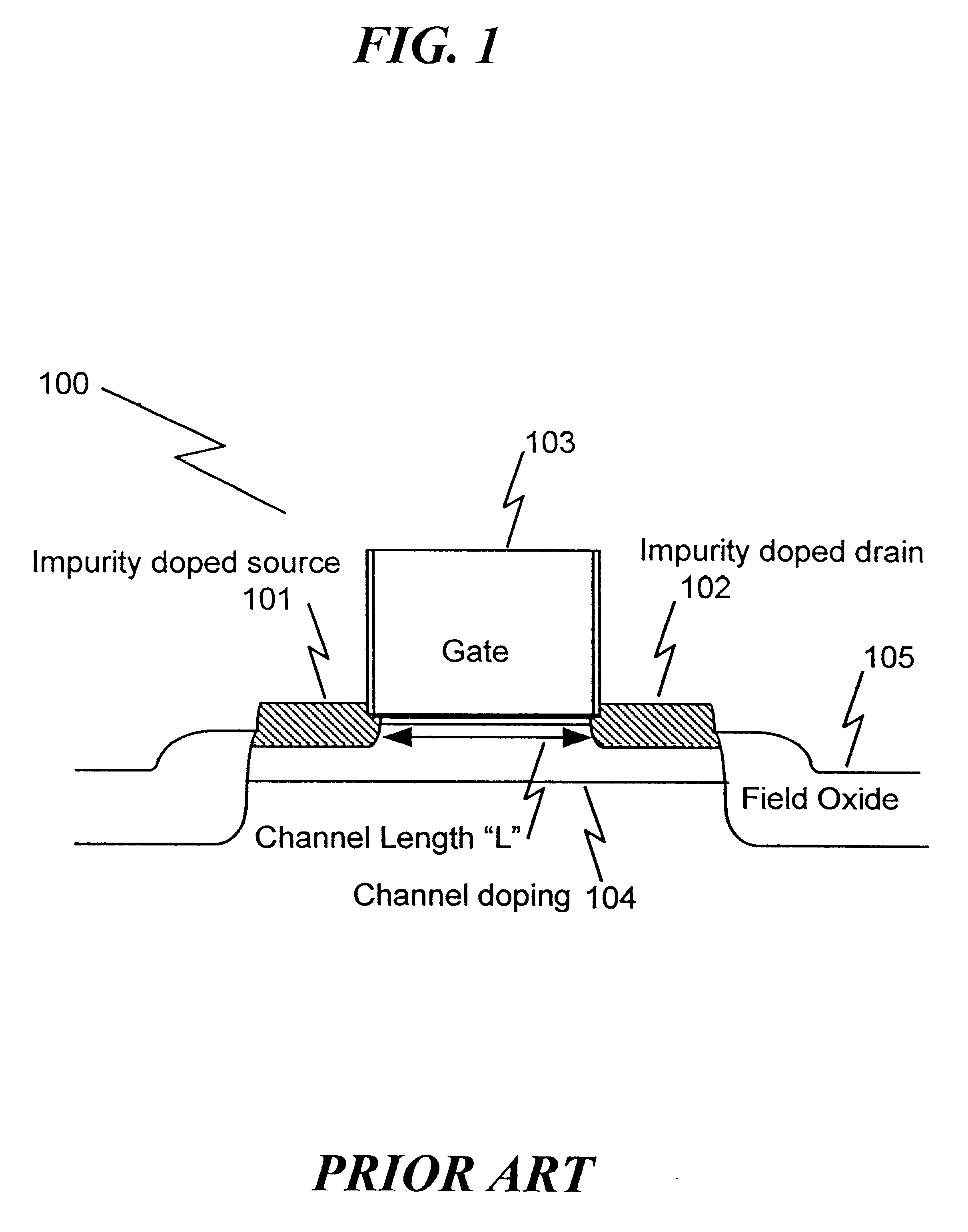
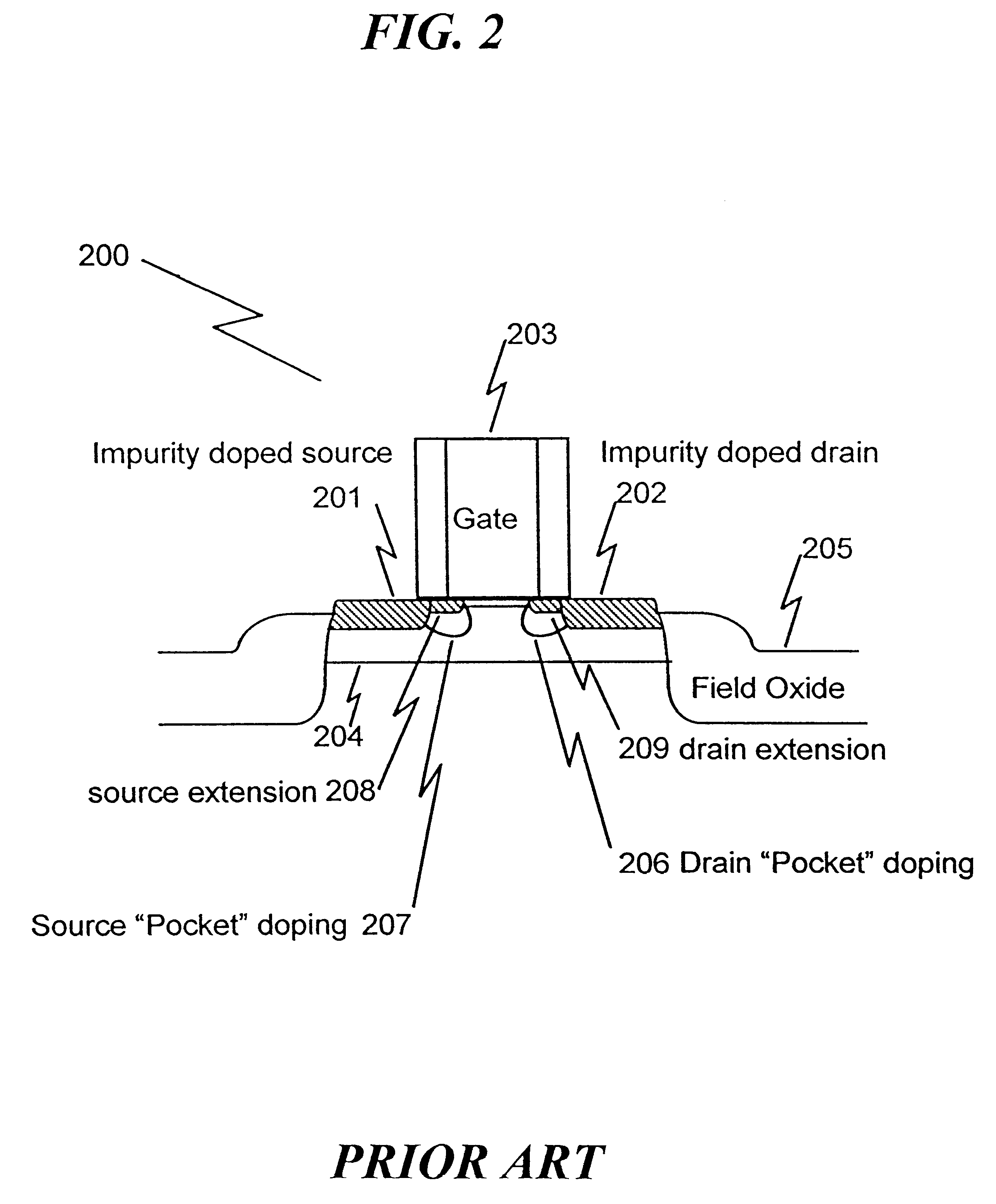
- Description
- Claims
- Application Information
AI Technical Summary
Benefits of technology
Problems solved by technology
Method used
Image

Examples
Embodiment Construction
Embodiments are Exemplary
While this invention is susceptible of embodiment in many different forms, there is shown in the drawings and will herein be described in detailed preferred embodiment of the invention with the understanding that the present disclosure is to be considered as an exemplification of the principles of the invention and is not intended to limit the broad aspect of the invention to the embodiment illustrated.
The numerous innovative teachings of the present application will be described with particular reference to the presently preferred embodiments, wherein these innovative teachings are advantageously applied to the particular problems of a MOSFET DEVICE SYSTEM AND METHOD. However, it should be understood that these embodiments are only examples of the many advantageous uses of the innovative teachings herein. In general, statements made in the specification of the present application do not necessarily limit any of the various claimed inventions. Moreover, some...
PUM
 Abstract
Description
Claims
Application Information
 - R&D
- Intellectual Property
- Life Sciences
- Materials
- Tech Scout
- Unparalleled Data Quality
- Higher Quality Content
- 60% Fewer Hallucinations
Browse by: Latest US Patents, China's latest patents, Technical Efficacy Thesaurus, Application Domain, Technology Topic, Popular Technical Reports.
© 2025 PatSnap. All rights reserved.Legal|Privacy policy|Modern Slavery Act Transparency Statement|Sitemap|About US| Contact US: help@patsnap.com