Optical formation device and method

Inactive Publication Date: 2001-01-30
NABLESCO CORP +1
View PDF5 Cites 86 Cited by
  • Summary
  • Abstract
  • Description
  • Claims
  • Application Information

AI Technical Summary

Benefits of technology

The size of the light spot irradiated on the exposure region from a light spot generator in the solid model creation apparatus of the present invention is not as small as an exposure region pixel, but rather is larger than the pixel. Furthermore, because exposure of each pixel is carried out in multiple fashion using a sum total plurality of light spots, the output of each light spot generator may be relatively low. It is therefore not necessary that a conventional large and expensive gas laser generator be employed as light source in the light spot generator, it being possible to employ a small and inexpensive solid-state luminescent element such as an LED therefor. As a result, it is possible to provide a solid model creation apparatus that is far more inexpensive than was the case conventionally (e.g., on the order of several millions of yen as opposed to several tens of millions of yen, as was the case conventionally).
As described above, in arraying a plurality of light spots at a small first pitch, a plurality of light spot generator subarrays, each comprising two or more light spot generators lined up in a single row in the primary scan direction at a second pitch which is the same as or greater than the light spot diameter may be provided, and these light spot generator subarrays may themselves be arranged in the secondary scan direction with a displacement therebetween in the primary scan direction which is equal to the aforesaid first pitch. Adoption of such an arraying method makes it possible for large light spot generators to be arrayed in the primary scan direction at the first pitch even when the size of each of those light spot generators is much larger than the first pitch.
In order to permit the aforementioned multiple exposure, a control apparatus may control the exposure apparatus as follows. To wit, the control apparatus first receives data indicating the cross-sectional profile of a solid model and expands the cross-sectional profile by applying a prescribed offset to this data. Next, while light spot generator(s) are scanning the exposure region, the control apparatus turns on light spot generator(s) for which the center of the light spot(s) therefrom are located at respective pixels contained within the expanded cross-sectional profile. A method incorporating this offset expansion processing makes it possible to carry out effective multiple exposure of all pixels within the cross-sectional profile of a solid model (in particular, not just the pixels at the interior of the profile but also pixels in the vicinity of the outline thereof) by merely carrying out a simple light spot drive method wherein respective light spot generators are turned on and off in accordance with the value of the pixel at the center of the light spot therefrom.
As mentioned above, a solid-state luminescent element such as an LED may be employed as light source in the respective light spot generators. It is desirable that the apparatus permit a constitution wherein an optical fiber is connected to each LED, and that a light spot from the tip of that optical fiber irradiate the plane of exposure. It is further desirable that the apparatus permit a constitution wherein a GRIN lens (gradient index lens; graded refractive index lens) is arranged at the end of the tip of the optical fiber, and the image of the tip of the optical fiber is formed on the exposure region. Such a constitution will make it possible to produce a light spot having a small diameter corresponding to the diameter of the optical fiber (e.g., 0.5 mm). Use of a light spot on this order of smallness will permit creation of solid models having dimensional accuracies adequately permitting practical use for typical solid model creation applications. In addition, the solid model creation apparatus of the present invention possesses an extremely large practical advantage because price is lowered to the extent that it is of a different order of magnitude in comparison with conventional solid model creation apparatuses employing gas lasers, and because the apparatus is also made small in size.
The present invention also provides a solid model creation method. In this method, while a photocurable resin exposure region is being scanned by at least one light spot larger in size than a pixel therein, a light spot capable of irradiating a selected pixel is turned on, as a result of which a sum total plurality of light spots are directed at the selected pixel and multiple exposure is carried out. Such a method permits practical solid model creation to be carried out using a light spot generator that, for example as with the aforementioned combination of LED and optical fiber, while capable of generating only a light spot larger than a pixel and wherein moreover light spot output is small, is nonetheless small in size and extremely inexpensive.

Problems solved by technology

In addition, the gas laser generator is itself expensive, and moreover, depending on the type of generator, a 200 V power supply and a water cooling apparatus (chiller) may well be required.
Accordingly, the price of a conventional solid model creation apparatus is extremely high (e.g., several tens of millions of yen).
Furthermore, because exposure of each pixel is carried out in multiple fashion using a sum total plurality of light spots, the output of each light spot generator may be relatively low.

Method used


Image

  • Optical formation device and method
  • Optical formation device and method
  • Optical formation device and method

Examples


Embodiment Construction

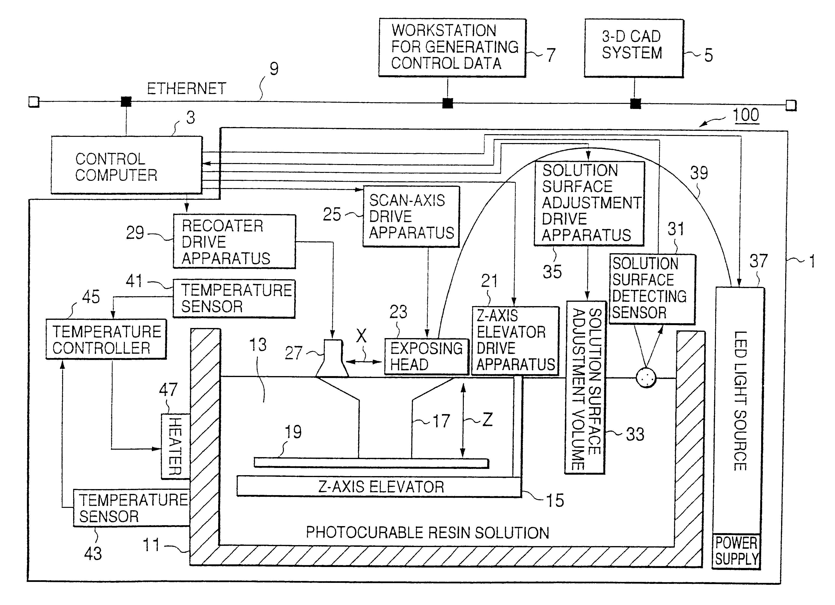
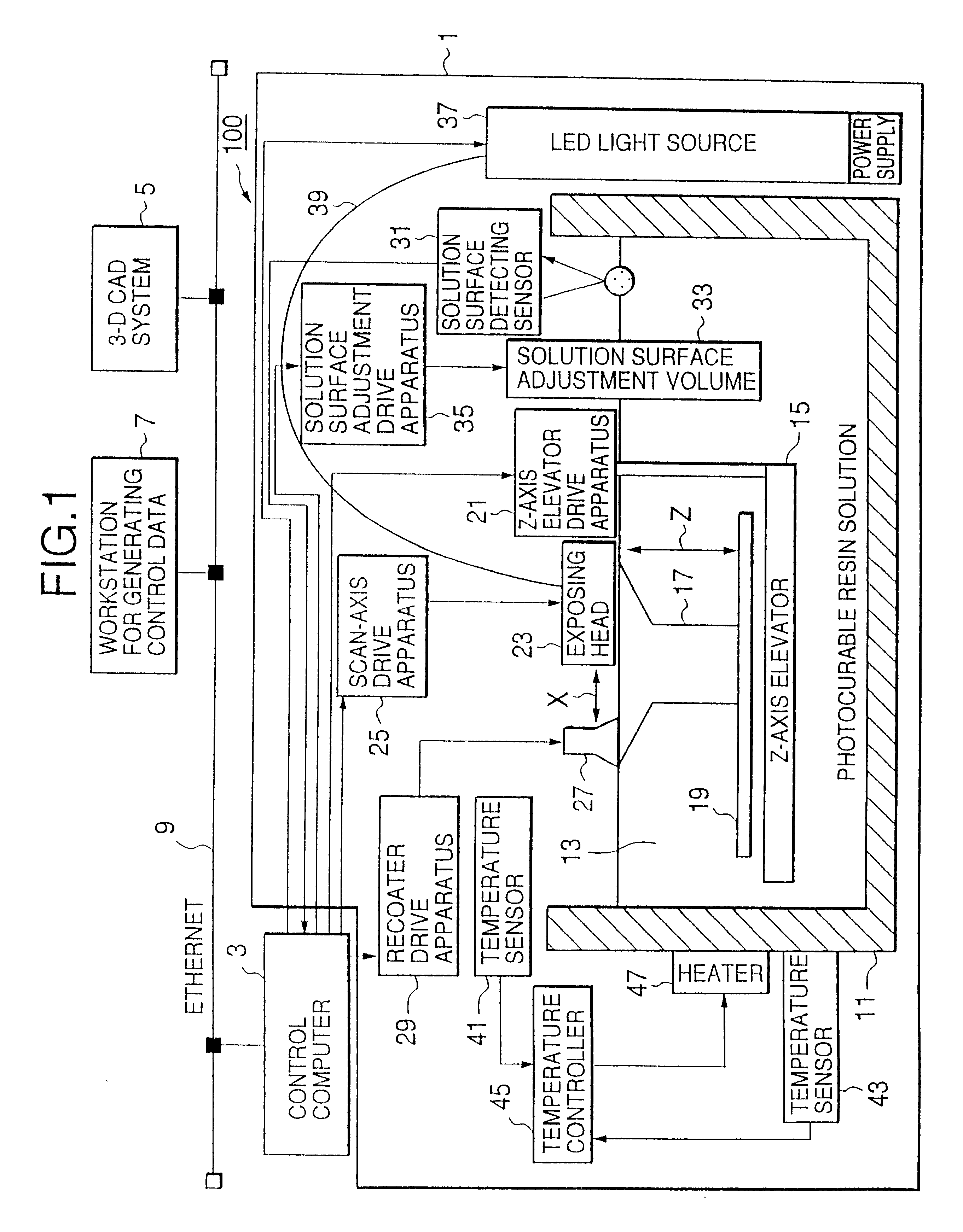
FIG. 1 shows the overall constitution of a solid model creation apparatus associated with an embodiment of the present invention.

This solid model creation apparatus 100 possesses an apparatus main body 1 comprising mechanisms necessary for solid model creation, a light source, and drive apparatuses therefor; and a control computer 3 for controlling operation of this main body 1. The control computer 3 may be connected by way of "Ethernet" or other such telecommunications network 9 to a three-dimensional CAD system 5, a workstation 7 for generation of control data, and so forth. The three-dimensional CAD system 5 performs three-dimensional modeling of a solid model and generates three-dimensional profile data for the solid model. The workstation 7 for generation of control data slices this three-dimensional profile data into a multiplicity of thin layers, generates a two-dimensional profile for each layer, and supplies this two-dimensional profile data for each layer, thickness data,...


PUM

PropertyMeasurementUnit
Sizeaaaaaaaaaa
Diameteraaaaaaaaaa
Sizeaaaaaaaaaa

Abstract

The purpose of the invention is to provide a solid model creation apparatus that is small in size and inexpensive. A multiplicity of blue LEDs are prepared, optical fibers are connected thereto, and GRIN lenses are arranged at the ends of the tips of the respective optical fibers to constitute an exposing head 23. The exposing head 23 forms images of the end faces of the respective optical fibers in a photocurable resin exposure region 24 as light spots 55. The diameter of a light spot 55 is, for example, 0.5 mm, but the size of a pixel 71 within the exposure region 24 is much smaller; for example, 62.5mu. The multiplicity of optical fibers at the exposing head 23 are arrayed in a matrix such that they are displaced in staggered fashion so that respective light spots 55 are lined up at the pitch 62.5mu of the pixels 71 in the primary scan (Y-axis) direction. As the exposing head 23 scans the exposure region 24 in the secondary scan (X-axis) direction, all of the light spots capable of directing light onto appropriate pixels, these being the respective pixels 71 to be cured within the exposure region 24, are turned on and multiple exposure is carried out.

Description

The present invention pertains to a solid model creation apparatus for creating models having three-dimensional shapes using photocurable resin.TECHNICAL BACKGROUNDA great many inventions are known with respect to solid model creation apparatuses, these including, for example, Japanese Patent No. 1827006. Conventional solid model creation apparatuses generally employ as light source a gas laser generator outputting ultraviolet laser light.Gas laser generator size is fairly large (e.g., 150 cm.times.30 cm.times.30 cm), and consequently solid model creation apparatus main body size is likewise correspondingly large. In addition, the gas laser generator is itself expensive, and moreover, depending on the type of generator, a 200 V power supply and a water cooling apparatus (chiller) may well be required. Accordingly, the price of a conventional solid model creation apparatus is extremely high (e.g., several tens of millions of yen).Accordingly, the object of the present invention is to...

Claims


Application Information

Patent Timeline
IPC IPC(8): B29C35/08B29C41/02B29C67/00B29C69/00B29K105/24
CPCB29C67/0066B29K2995/0073B29C64/135B29C67/00
Inventor ARAI, MAHITONIINO, TOSHIKINAKAGAWA, TAKEO
Owner NABLESCO CORP
Why Eureka
Try Eureka