In situ Etching of inorganic dielectric anti-reflective coating from a substrate

Inactive Publication Date: 2000-08-15
APPLIED MATERIALS INC
View PDF7 Cites 33 Cited by
  • Summary
  • Abstract
  • Description
  • Claims
  • Application Information

AI Technical Summary

Benefits of technology

A feature of the present invention is the ability to etch a dielectric ARC with high etch selectivity. Another feature of the present invention is the capability of in situ etching of dielectric layers and inorganic ARC's. An advantage of present invention is that accurate etching of the DARC layer is produced. Another advantage of present invention is that the substrate being processed does not need to be removed from the processing chamber. Yet another advantage of present invention is that unwanted etching of layers underlying the layer being patterned is avoided. Another advantage of the present invention is that it can be used for all work related to etching, such as metal and silicon etching.
is that it can be used for all work related to etching, such as metal and silicon etching.

Problems solved by technology

Errors in these dimensions can result in variations in device characteristics or open- / short-circuited devices, thereby adversely affecting device yield.
This uneven topology can cause reflection and refraction of the monochromatic light, resulting in exposure of some of the photoresist beneath the opaque portions of the mask.
As a result, this uneven surface topology can alter the mask pattern transferred to the photoresist layer, thereby altering the desired dimensions of the structures subsequently fabricated.
In such a situation, the reflected light interferes with the incident light and causes a periodic variation in light intensity within the photoresist layer in the vertical direction.
The existence of standing waves in the photoresist layer during exposure causes roughness in the vertical walls formed when sections of the photoresist layer are removed during patterning, which translates into variations in linewidths, spacing and other critical dimensions.
However, portions of the DARC must be etched during fabrication of the device, which is currently a challenge.
While a small amount of the first layer is normally removed in such situations, extremely low etch selectivity may permit substantial etching of the first layer.
However, currently, typical etch selectivities for DARCs are very low.
Thus, typical reactive ion etching processes used to selectively etch thin film patterning layers of a device do not work well with DARCs due to the poor etch selectivities.
As a result, currently, DARCs do not produce results that they are potentially capable of producing.
In addition, currently, etching of DARCs are not performed in situ (same chamber without intervening processing steps, such as cleanings, etc.), which cause inefficiencies and reduces throughput.
Consequently, DARCs are not commercially viable because the etching of a DARC is expensive, time consuming, and inefficient.
Hence, the results produced by DARCs are not worth the time and costs incurred.

Method used


Image

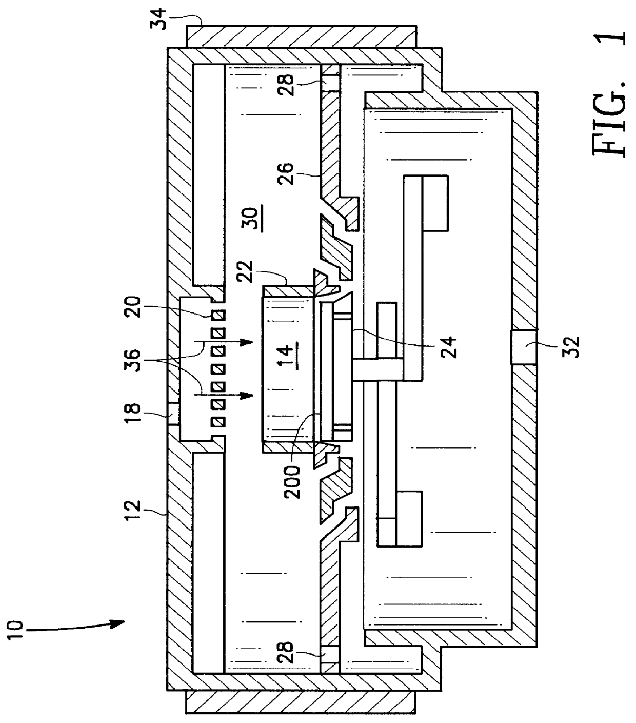
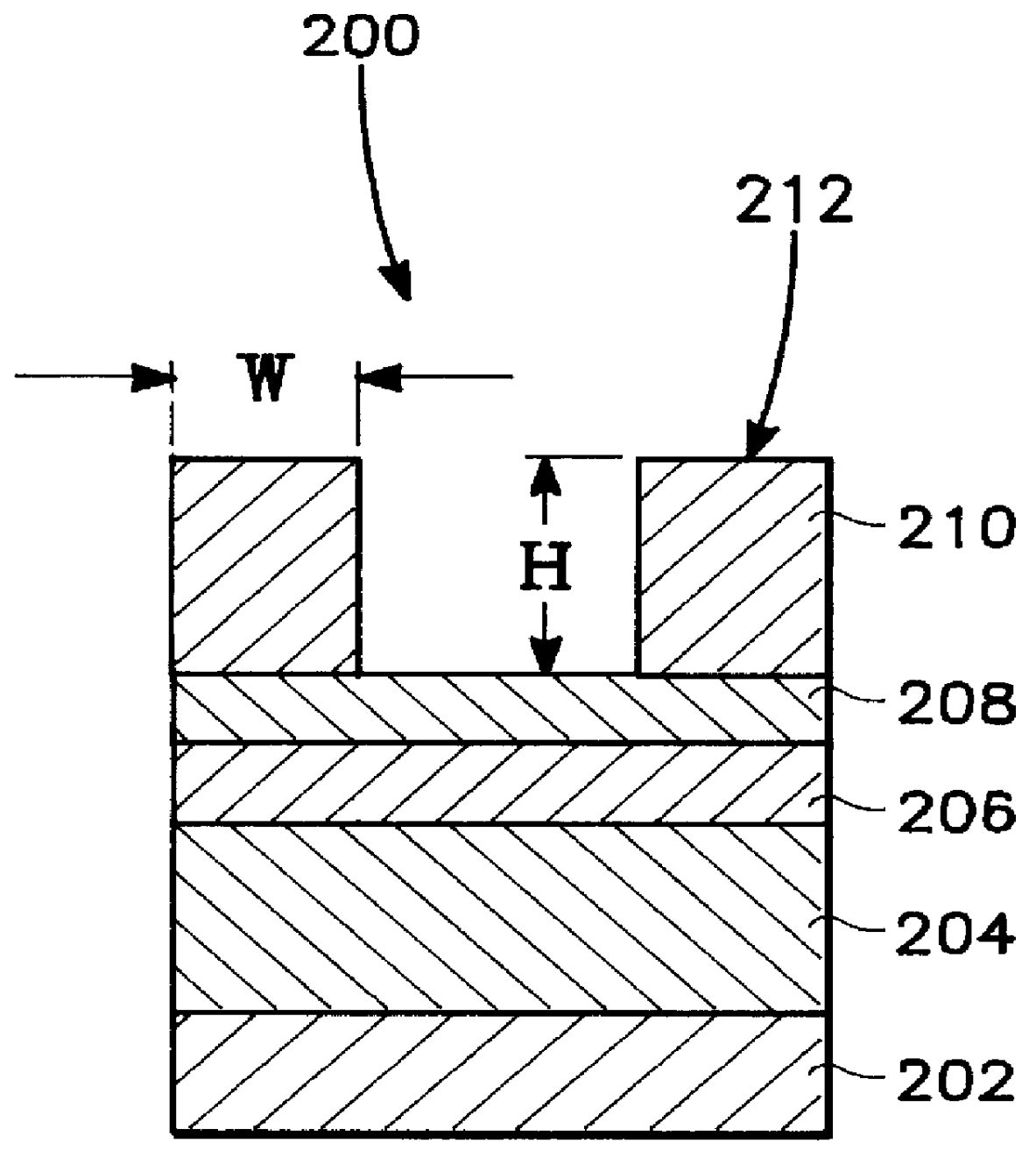
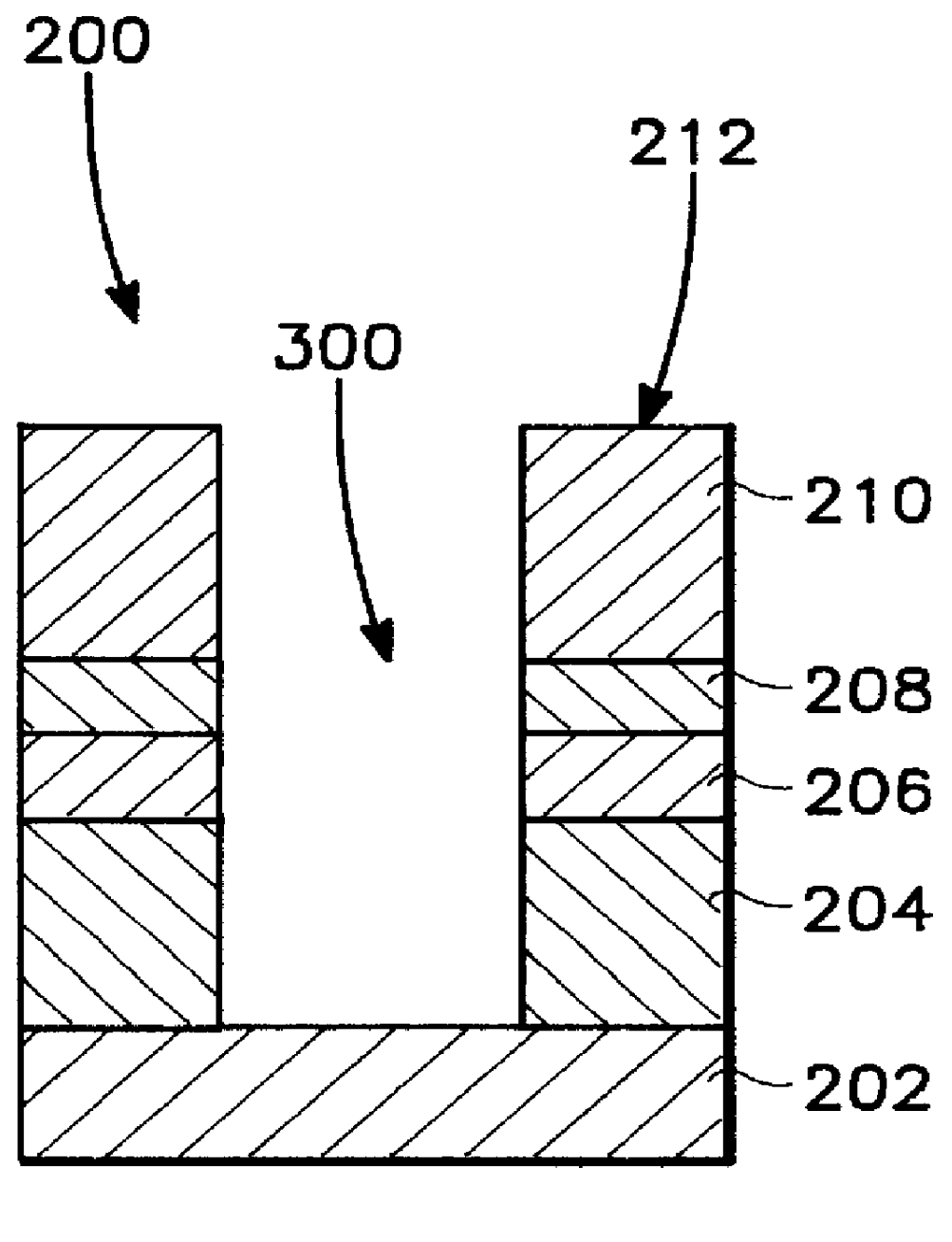
  • In situ Etching of inorganic dielectric anti-reflective coating from a substrate
  • In situ Etching of inorganic dielectric anti-reflective coating from a substrate
  • In situ Etching of inorganic dielectric anti-reflective coating from a substrate

Examples


working example 2 (

Poly Gate Etch--Doped):

DARC Open: 75CF.sub.4 / 5He--O.sub.2 / 4mT / 250Ws / 25Wb / Endpoint+20% / 50.degree. C.

Poly ME: 60Cl.sub.2 / 120HBr / 10He--O.sub.2 / 6mT / 600Ws / 100Wb / EP

Poly OE: 160HBr / 10He--O.sub.2 / 50mT / 750Ws / 100Wb / 30s

RESULTS: Vertical Poly profile, no microloading

Remaining G.sub.ox =82 .ANG. (Pre), 66 .ANG. (post-dip)

working example 3 (

Poly Gate Etch--Silicide on top of Poly):

DARC Open: 75CF.sub.4 / 5He--O.sub.2 / 4mT / 250Ws / 25Wb / Endpoint+20% / 50.degree. C.

WSix: 130Cl.sub.2 / 5He--O.sub.2 / 8mT / 600Ws / 130Wb / EP+30%

Poly ME: 30Cl.sub.2 / 120HBr / 10He--O.sub.2 / 8mT / 600Ws / 100Wb / Endpoint

Poly OE: 160HBr / 10He--O.sub.2 / 50mT / 750Ws / 100Wb / 30s

RESULTS: Good profiles, very little microloading

Remaining G.sub.ox =92 .ANG. (Pre), 76 .ANG. (post-dip)

The process conditions used for all three working examples are set forth TABLE I below. The etch selectivities are set forth in TABLE II below, and some results are set forth in TABLE III below. It should be noted that the working examples are given for illustrative purpose only.

TABLE II

TABLE III

The results of the above working examples demonstrate that a process according to the invention provides a high degree of anisotropic etching, substantially no undercutting or notching, a high selectivity of the DARC layer to polysilicon, and very low critical dimension loss.


PUM


Abstract

The present invention is embodied in a method and apparatus for etching dielectric layers and inorganic ARC's without the need for removing the substrate being processed from the processing chamber and without the need for intervening processing steps such as chamber cleaning operations (in situ process). A layer and / or a multi-layer film deposited on a substrate, such as silicon, is located within a processing chamber. The substrate has a base, an underlying layer above the base, an overlying layer above the underlying layer, and a top dielectric anti-reflective coating (DARC) layer formed on the overlying layer. In the preferred method, first, the DARC layer and the overlying layer is etched by a first process gas. Next, the underlying layer is etched by a second process gas.

Description

1. Field of the InventionThe present invention relates in general to an apparatus for, and the processing of, semiconductor substrates. In particular, the invention relates to the in situ etching of dielectric anti-reflective coatings during substrate processing.2. Related ArtThe critical dimensions (CD's) and geometries of semiconductor devices have decreased dramatically in size since they were first introduced several decades ago. Although, currently, most semiconductor devices are fabricated with feature sizes of about 0.35 microns, it is desirable to produce semiconductor devices, for example, semiconductor integrated circuit chips, with smaller feature sizes, such as 0.25 microns and lower.One important micro geometry of such semiconductor devices includes the formation of a patterned thin film on a base substrate of the device by chemical reaction of gases. When patterning the thin films, it is desirable that fluctuations in line width and other critical dimensions be minimiz...

Claims


Application Information

Patent Timeline
IPC IPC(8): H01L21/02H01L21/027H01L21/3213H01L21/311
CPCH01L21/0276H01L21/31116H01L21/32137H01L21/32139
Inventor KUMARCHINN, JEFFREY D.
Owner APPLIED MATERIALS INC
Why Eureka
Try Eureka