Hot melt compositions with improved etch resistance

a technology of etch resistance and composition, applied in the direction of film/foil adhesive, circuit mask, nuclear engineering, etc., can solve the problems of reducing the density and definition of electrically conductive circuitry, affecting the etch resistance of hot melt composition, etc., to achieve good image definition and low flow

Active Publication Date: 2015-02-26
ROHM & HAAS ELECTRONICS MATERIALS LLC
View PDF3 Cites 5 Cited by
  • Summary
  • Abstract
  • Description
  • Claims
  • Application Information

AI Technical Summary

Benefits of technology

The patent text discusses the use of hot melt compositions for etching copper in PCB manufacturing. These compositions can also be used to resist etching of inner layers. Ammoniacal etchants are preferred over acidic etchants as they are less harmful and can protect the protected copper portions on the circuitry. The use of a single etchant for both inner and outer layers eliminates the need for two etch modules.

Problems solved by technology

Although the process is widely used in the manufacture of PCBs it is tedious, expensive and wasteful of materials since the photoresist layer is made separately and applied over the total area of the copper / dielectric substrate laminate.
Furthermore, the photo-tool containing the negative image of the desired electrically conductive circuitry is often distanced from the photo-tool layer such that diffraction of UV light irradiation occurs and leads to development and polymerization in areas of the photoresist not directly beneath the UV transparent areas of the photo-tool.
Such problems must be taken into consideration when preparing photo-tools and may reduce the density and definition of the electrically conductive circuitry.
The density and integrity of the intended electrically conductive circuitry can be seriously compromised if either the unexposed photoresist is incompletely removed or if some of the exposed and polymerized photoresist is removed prior to chemically etching the copper.
If hot melt residue is left on a substrate after removal, the residue may compromise further processing of the substrate.
Any residue remaining on the PCB after stripping may compromise metal plating resulting in a defective electronic device.
A major problem which often arises during formation of the circuitry is undercutting.
This results in defective and inefficient PCBs.
This problem is common when the circuits are formed using an etching method in combination with a mask.
Upon application of the etch to the selectively masked substrate the etch may not only remove portions of the substrate not covered by the mask but by capillary action seep under the mask at the interface of the mask and the substrate causing portions of the substrate covered by the mask to be undesirably etched away.
This results in circuitry having irregular widths which results in irregular and non-uniform current flow.
In addition, such undercutting may form tributaries which adjoin adjacent current lines resulting in electrical shorts.
Etching at high pH can cause chemical attack of some etch resists resulting in an unacceptable large undercut or lifting off of layers from the substrate caused by a combination of capillary undercut of the etching chemistry and etchants penetrating into the resist causing swelling and adhesion failure.
As the industry seeks to manufacture electrical devices using thinner and more delicate circuitry and at the same time increase the plurality of circuits to increase electrical out-put, the foregoing problems become compounded by difficulty of working with smaller and more delicate materials.

Method used


Image

  • Hot melt compositions with improved etch resistance
  • Hot melt compositions with improved etch resistance
  • Hot melt compositions with improved etch resistance

Examples


examples 1-4

[0067]The following inkjet etch resist compositions were prepared:

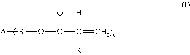
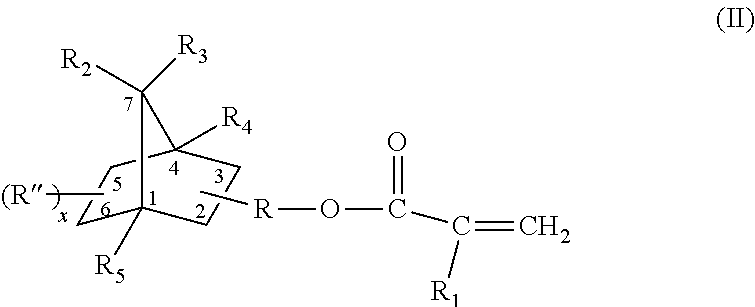
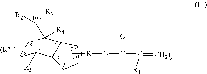
Formulation1234MonomersIsobornyl acrylate48 wt %Dicyclopentadienyl50 wt %50 wt %methacrylateTrimethylolpropane triacrylate17 wt %Polybutadiene diacrylate10 wt %Polybutadiene dimethacrylate12 wt %Tricyclodecane dimethanoldiacrylate60 wt %Aliphatic urethane acrylate113 wt %PlasticizersPartially hydrogenated rosinresin220 wt %Hydrogenated rosin resin320 wt %Liquid rosin420% PhotoinitiatorsIsopropyl thixanthone 5 wt % 5 wt %2%2.5 wt % Hydroxycylohexyll phenyl 5 wt % 5 wt %3%2.5 wt % ketoneWaxesCeresin wax10 wt %7.5 wt % Candelilla wax10 wt %Esterified Montan wax10 wt %Montan wax7.5 wt % Myristic acid10%Palmitic acid10 wt %Stearic acid 5 wt %1EBECRYL ® 8309 Acrylic Ester from Cytec Industries2STAYBELITE ® A typical composition and properties: abietic acid 3Hercolyn Floral AX-E from Pinova solutions inc.4Hercolyn D- Methyl Hydrogenated Rosinate from Pinova solutions inc.

[0068]All the formulations were prepared by the same m...

example 5

Etch Resist for PCB Application

[0069]The resist compositions from examples 1-4 were selectively ink jetted from a piezoelectric drop-on-demand print head (Spectra™ SE-128) onto four separate copper clad FR4 / glass epoxy panels at a thickness of 15 μm to 30 μm. The temperature during inkjetting was from 85° C. to 95° C. After the resist compositions were selectively applied to their respective panels, the compositions were exposed to UV light varying from 150-1000 mJ / cm2 using a Fusion D lamp running at 120 W / cm. All the resists cured.

[0070]The hardness of each cured resist is tested using the AS™ D3363-05 pencil hardness test, 5H being the hardest and 1H being the softest. The hardness value for each cured resist was measured to be 4H.

[0071]Each panel was then passed through a conventional etching module containing a commercial ammonia etchant which was a mixture of 5-15% of each of NH4OH and NH4Cl at pH 8.9, 52° C. for 5 min. The copper was etched to a depth of 105 μm. The resist co...

example 6

Etch Resist for Semiconductor Applications

[0073]Solar cells having mono-crystalline or poly-crystalline silicon wafers, a p / n junction and coated with a silicon nitride anti-reflective layer on the front side were provided. Each of the four resist compositions in Examples 1-4 were selectively coated on the anti-reflective layers by inkjet Each resist was applied to one of the two types of silicon wafers. The resists were then exposed to UV light of 150-1000 mJ / cm2 to cure the resists.

[0074]Each solar cell was then immersed in a 20% solution of hydrofluoric acid at 30° C., pH=1 for 5 minutes to etch away the uncoated silicon nitride and expose the n+ doped surface of the silicon. The solar cells were then rinsed with tap water for 2 minutes and air dried. An optical microscope was used to observe the cured resist on each solar cell. There was no observable loss of cured hot melt on either solar cell. The cured hot melt appeared to have resisted the acid etch. Each wafer was then dipp...


PUM

PropertyMeasurementUnit
Massaaaaaaaaaa
Massaaaaaaaaaa
Acidityaaaaaaaaaa

Abstract

Hot melt compositions include non-aromatic cyclic (alkyl)acrylates and low acid number waxes. Upon application of actinic radiation, the hot melt compositions cure to form resists. They may be stripped from substrates with high alkaline strippers. The hot melt compositions may be used in the manufacture of printed circuit boards and photovoltaic devices.

Description

FIELD OF THE INVENTION [0001]The present invention is directed to hot melt compositions with improved etch resistance. More specifically, the present invention is directed to hot melt compositions with improved etch resistance containing non-aromatic cyclic (alkyl)acrylates and low acid number waxes.BACKGROUND OF THE INVENTION[0002]Hot melts are in solid phase at ambient temperatures, but exist in liquid phase at elevated operating temperatures in inkjet printing devices. At the inkjet operating temperatures droplets of liquid hot melt are ejected from the printing device and, when the droplets contact a surface of a printing material, they harden to form a predetermined pattern of droplets.[0003]Hot melts have been employed in direct and transfer printing processes. Hot melts are typically cast into solid sticks and placed into an inkjet printing device. The temperature of the inkjet device is raised to an operating temperature where a liquid phase with selective fluid properties i...

Claims


Application Information

Patent Timeline
IPC IPC(8): C09D11/34H05K3/06H05K3/18B05D3/06
CPCC09D11/34B05D3/06H05K3/18H05K3/061H05K3/06C09D11/101C09D11/12C09D11/38H05K3/0023H05K3/0076H05K3/0079H05K3/0082H05K2203/013H05K2203/0545H05K2203/0769H05K2203/0793H05K2203/122C09D11/107C09D133/08C09D133/10C09D135/02H05K3/002H05K3/181
Inventor BALANTRAPU, KRISHNABARR, ROBERT K.
Owner ROHM & HAAS ELECTRONICS MATERIALS LLC
Why Eureka
Try Eureka