Substrate for mounting element and process for its production

a technology of mounting elements and substrates, applied in the direction of manufacturing tools, conductive pattern formation, semiconductor/solid-state device details, etc., can solve the problems of deterioration of resin substrates, substantial increase in production costs, and failure to pass sulfurization tests, etc., to achieve excellent sulfurization resistance and good plating properties

Active Publication Date: 2014-07-24
ASAHI GLASS CO LTD
View PDF5 Cites 1 Cited by
  • Summary
  • Abstract
  • Description
  • Claims
  • Application Information

AI Technical Summary

Benefits of technology

[0020]According to the present invention, the thick conductor layer made of a metal such as silver (Ag) or copper (Cu) formed on the surface of the inorganic insulating substrate, is planarized (smoothed) by the wet blast treatment, and spaces among the thick conductor (Ag) particles are filled and the surface roughness Ra is adjusted to be at most 0.02 μm, whereby the plating property is good, and the thick conductor surface can be completely covered even by a Au-plated layer having a usual thickness. Thus, it is possible to obtain a substrate for mounting element, which is excellent in sulfurization resistance.

Problems solved by technology

However, such a resin substrate is likely to be deteriorated by a heat or light accompanying higher brightness of a LED element.
However, in recent years, a substrate to mount a LED element or the like, is required to have sulfurization resistance, and with conventional plated thicknesses (Ni-plated thickness of from 3 to 5 μm / Au-plated thickness of from 0.1 to 0.3 μm) required for the wiring bonding portions, there has been a problem that a color change to black is observed at the Ni / Au-plated portion in a sulfurization test in accordance with JIS-C-60068-2-43, thus failing to pass the sulfurization test.
However, the method of forming a thick Au layer or increasing the thickness of the Au-plated layer has had a problem that the production cost increases substantially.
Further, in the case of the LTCC substrate, there has been a problem such that if the sintering property is improved by reducing the particle size of the Ag powder, timing in shrinkage by firing will not meet with the substrate whereby the substrate is likely to undergo warpage.
However, by this method, it was not possible to increase the sulfurization resistance by removing the grain boundary void spaces or surface irregularities of the thick conductor (Ag) layer.
That is, although Patent Document 1 does not disclose the conditions for the wet blast treatment in detail, the blast treatment to remove glass is one to break and remove glass as a hard substance in a short time by blasting.
Under blast treatment conditions for such a purpose, it has been difficult to fill spaces among the conductor (Ag) particles.

Method used


Image

  • Substrate for mounting element and process for its production
  • Substrate for mounting element and process for its production
  • Substrate for mounting element and process for its production

Examples


example 1

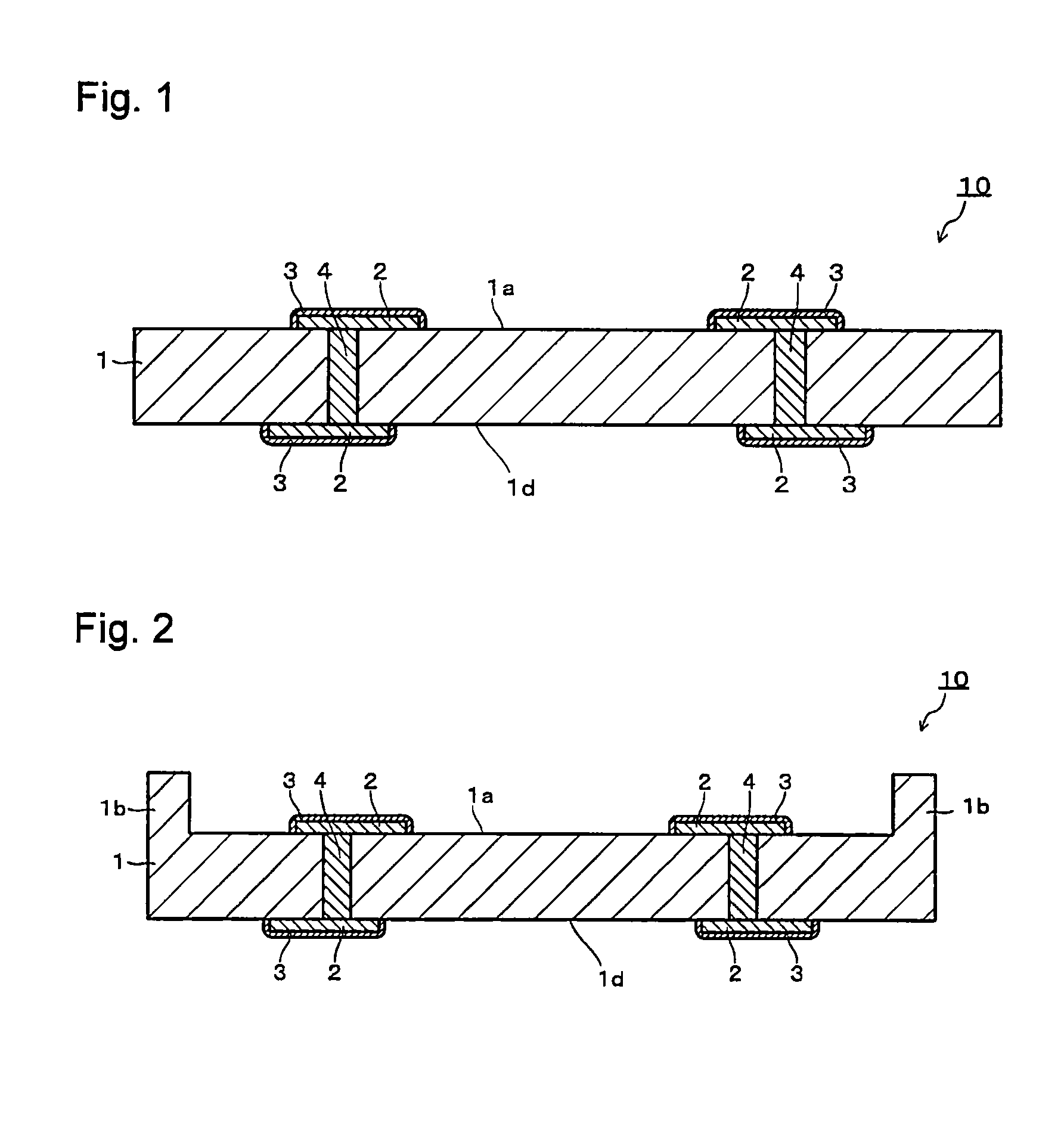
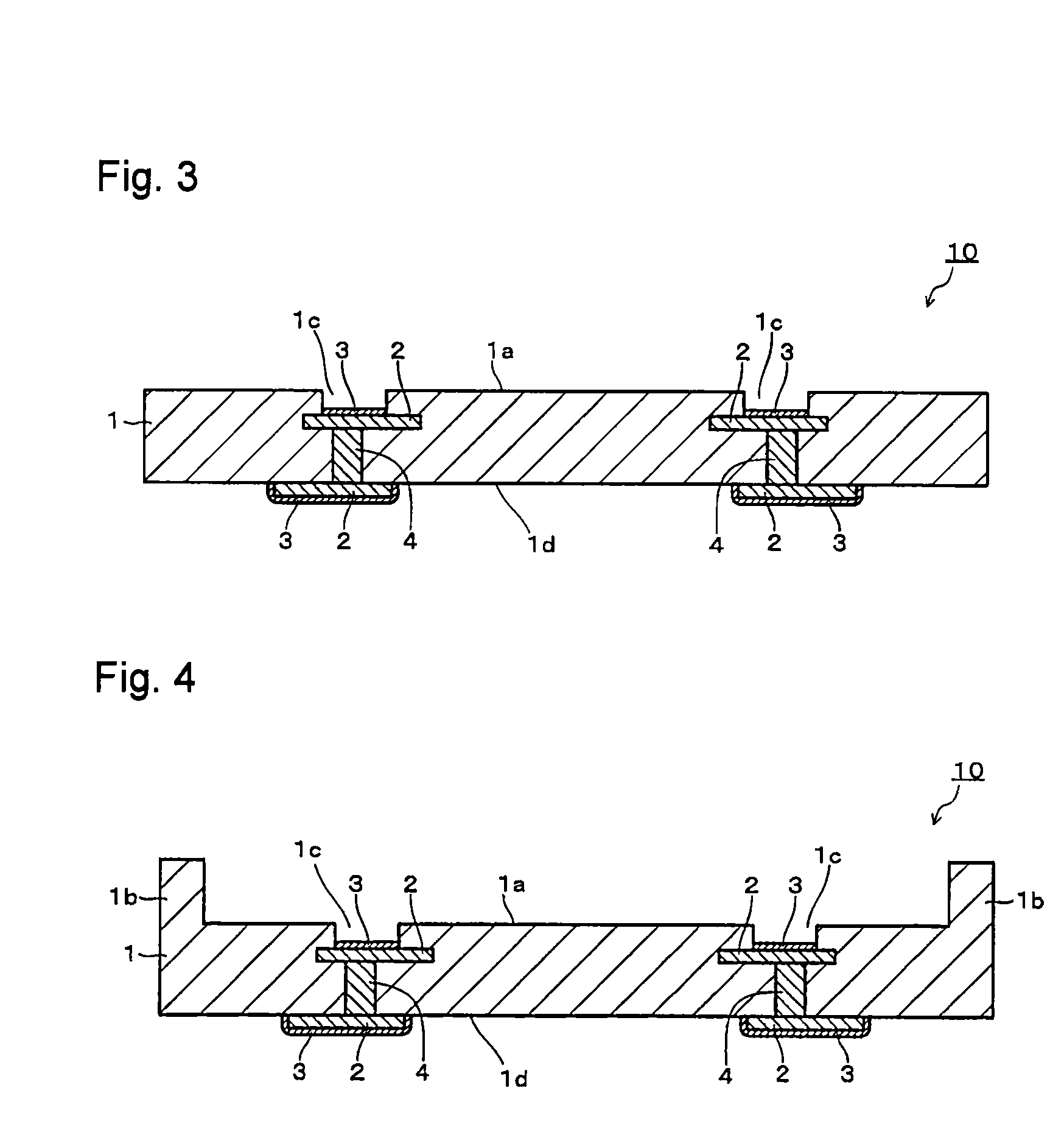
[0063]A substrate 10 for mounting element having a construction as shown in FIG. 1, provided with a LTCC substrate, was prepared.

[0064]Firstly, a glass ceramics green sheet for main body to prepare the substrate 10 for mounting element, was prepared. In the preparation, raw materials were blended and mixed so that SiO2 became 60.4 mol %, B2O3 15.6 mol %, Al2O3 6 mol %, CaO 15 mol %, K2O 1 mol % and Na2O 2 mol %, and this raw material mixture was put into a platinum crucible and melted at 1,600° C. for 60 minutes. Then, this molten state glass was cast and cooled. This glass was ground by a ball mill made of alumina for 40 hours to obtain a glass powder for substrate main body. Here, ethyl alcohol was used as the solvent at the time of grinding.

[0065]40 mass % of this glass powder for main body and 60 mass % of an alumina powder (tradename: AL-45H manufactured by Showa Denko K.K.) were blended and mixed to prepare a glass ceramics composition. To 50 g of this glass ceramics compositi...

example 2

[0073]A substrate 10 for mounting element having a construction as shown in FIG. 1, provided with a ceramics substrate, is prepared.

[0074]Firstly, a ceramics green sheet for main body to prepare the substrate 10 for mounting element, is prepared. In the preparation, firstly, 96 mass % of an alumina powder (tradename: AL-45H manufactured by Showa Denko K.K.) and 4 mass % of a sintering aid (a talc powder containing 65.8 mass % of SiO2 and 34.2 mass % of MgO) were blended and mixed to prepare a ceramics composition. To 50 g of this ceramics composition, 15 g of an organic solvent (a mixture of toluene, xylene, 2-propanol and 2-butanol in a mass ratio of 4:2:2:1), 2.5 g of a plasticizer (di-2-ethylhexyl phthalate), 5 g of polyvinyl butyral (tradename: PVK#3000K manufactured by DENKI KAGAKU KOGYO KABUSHIKI KAISHA) as a binder and a dispersing agent (tradename: BYK180 manufactured by BYK Japan KK)) are blended and mixed to prepare a slurry.

[0075]This slurry is applied on a PET film by a ...


PUM

PropertyMeasurementUnit
surface roughness Raaaaaaaaaaa
particle sizeaaaaaaaaaa
temperatureaaaaaaaaaa

Abstract

To provide a substrate for mounting element having sulfurization resistance improved by increasing planarity of the surface of a thick conductor layer.The substrate 10 for mounting element of the present invention has such a structure that on a surface of a LTCC substrate or ceramics substrate as an inorganic insulating substrate 1, a thick conductor layer 2 is formed as an element connection terminal. The thick conductor layer 2 is made of a metal composed mainly of silver (Ag) or copper (Cu) and formed by printing and firing a metal paste. This thick conductor layer has its surface planarized by wet blast treatment to a surface roughness Ra of at most 0.02 μm. A Ni / Au-plated layer 3 is formed on the thick conductor layer 2, so that the surface of the thick conductor layer 2 is completely covered without any space.

Description

CROSS-REFERENCE TO RELATED APPLICATIONS[0001]This application is a divisional of and claims the benefit of priority to U.S. Ser. No. 12 / 955,488, filed Nov. 29, 2010, which is based on and claims the benefit of priority to Japanese Patent Application No. 2010-018925, filed Jan. 29, 2010 and Japanese Patent Application No. 2010-203104, filed Sep. 10, 2010, including specifications, claims, drawings and summaries. The entire contents of these applications are incorporated herein by reference.TECHNICAL FIELD[0002]The present invention relates to a substrate for mounting element and a process for its production, particularly to a substrate for mounting element excellent in sulfurization resistance, wherein planarity of a surface of a thick conductor layer formed on the substrate surface is good, and a process for producing such a substrate.BACKGROUND ART[0003]In recent years, along with a tendency to a high brightness and whitening of a light-emitting diode (hereinafter referred to as LE...

Claims


Application Information

Patent Timeline
Patent Type & Authority Applications(United States)
IPC IPC(8): H05K3/30
CPCH05K3/30B24C3/322B24C7/0007H01L23/13H01L23/15H01L23/49827H01L2924/09701H01L2924/0002H01L33/62H05K1/0306H05K1/113H05K3/246H05K2201/0347H05K2201/09472Y10T29/49155H01L2924/00
Inventor NAKAYAMA, KATSUYOSHI
Owner ASAHI GLASS CO LTD
Why Eureka
Try Eureka