ECR-plasma source and methods for treatment of semiconductor structures
a technology of plasma source and semiconductor structure, applied in plasma technique, electrical apparatus, electric discharge tube, etc., can solve problems such as output power, noise factor and coefficient of efficiency, saturation current deterioration of principal transistor parameters,
- Summary
- Abstract
- Description
- Claims
- Application Information
AI Technical Summary
Benefits of technology
Problems solved by technology
Method used
Image
Examples
example 1
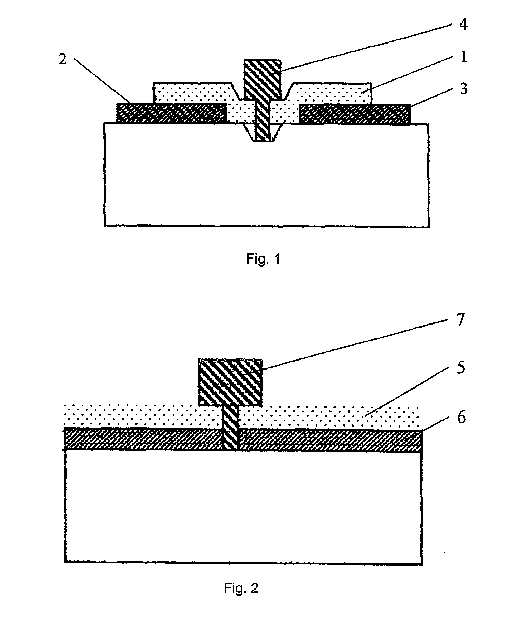
[0047]An epitaxial GaAs structure is used, which has been grown by gas epitaxy of organometallic compounds. Layers have been grown on semi-insulating GaAs substrate in following order: 0.5 micron of undoped GaAs buffer layer, 150 nm of active layer doped to 5·1017 cm−3, and 50 nm of contact layer with doping concentration of 5·1018 cm−3. Construction of T-shaped gate is shown schematically in FIG. 1, where:
[0048]1—silicon nitride layer;
[0049]2—source;
[0050]3—drain;
[0051]4—T-shaped gate.
[0052]Sequence of T-shaped gate production operations is as follows:
[0053]after etching of mesa-structures, optical lithography is performed for patterning of Ohmic contacts, sputtering of metals forming Ohmic contact, and firing of Ohmic contacts, and silicon nitride layer 100-120 nm thick is deposited using ECR-plasma enhancement,
[0054]0.2-0.4 micron thick layer of electron-beam resist is deposited and first electron-beam lithography is performed in order to form sub-100 nm part of the gate,
[0055]EC...
example 2
[0059]Construction of T-shaped line of metal wiring is shown schematically in FIG. 2, where:
[0060]5—layer of silicon nitride;
[0061]6—polyimide;
[0062]7—T-shaped conductor.
[0063]Sequence of production operations in manufacturing of T-shaped conductor is as follows:
[0064]polyimide layer having thickness required by technology is deposited on the substrate,
[0065]layer of silicon nitride 100-120 nm thick is grown using ECR-plasma enhancement,
[0066]layer of electron-beam resist 0.2-0.4 micron thick is deposited, and first electron-beam lithography is performed in order to pattern sub-100 nm part of the conductor,
[0067]ECR-plasma etching of silicon nitride is carried out in a mixture of CF4 and Ar (30 cm3 / min CF4, 20 cm3 / min Ar) at total pressure within reactor 3 mTorr, and ECR-plasma etching of polyimide in oxygen medium at pressure 1 mTorr,
[0068]layer of electron-beam resist 0.4 micron thick is deposited, and second electron-beam lithography is performed in order to form upper 600 nm par...
example 3
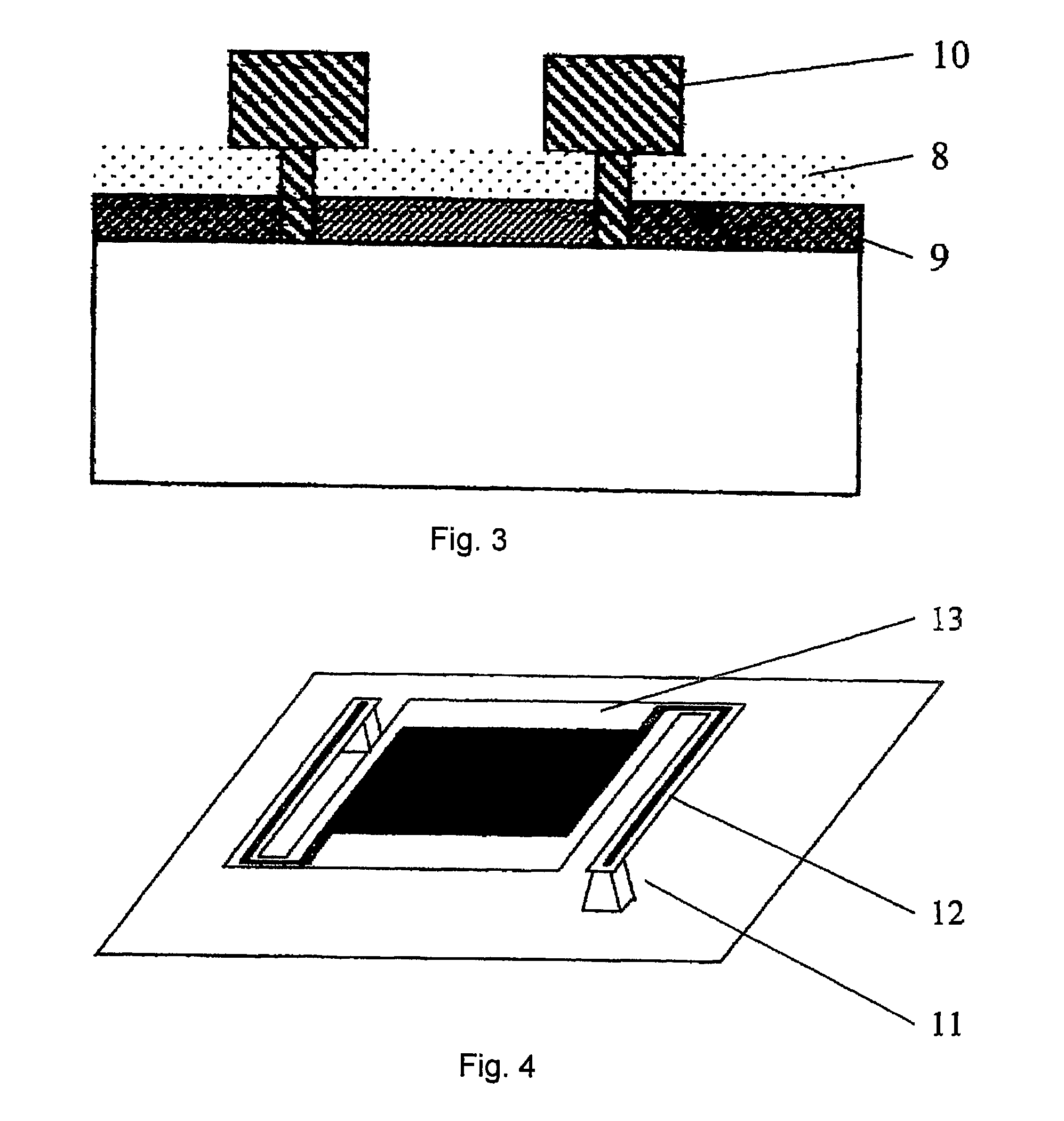
[0071]Construction of T-shaped microstrip lines having transverse dimension at base in sub-100 nm range is shown schematically in FIG. 3, where:
[0072]8—silicon nitride layer;
[0073]9—polyimide;
[0074]10—T-shaped microstrip lines.
[0075]Sequence of production operations during manufacturing of T-shaped microstrip lines having transverse dimensions at base in the sub-100 nm range is as follows:
[0076]polyimide layer 100-2000 nm thick is deposited on the substrate with active elements prefabricated,
[0077]layer of silicon nitride 100-120 nm thick is grown using ECR-plasma enhancement,
[0078]layer of electron-beam resist 0.2-0.4 micron thick is deposited, and first electron-beam lithography is performed in order to pattern sub-100 nm part of the conductor,
[0079]ECR-plasma etching of silicon nitride is performed in a mixture of CF4 and Ar (30 cm3 / min CF4, 20 cm3 / min Ar) at total pressure within reactor 3 mTorr, and ECR-plasma etching of polyimide—in oxygen medium at pressure 1 mTorr,
[0080]laye...
PUM
 Abstract
Description
Claims
Application Information
 - R&D
- Intellectual Property
- Life Sciences
- Materials
- Tech Scout
- Unparalleled Data Quality
- Higher Quality Content
- 60% Fewer Hallucinations
Browse by: Latest US Patents, China's latest patents, Technical Efficacy Thesaurus, Application Domain, Technology Topic, Popular Technical Reports.
© 2025 PatSnap. All rights reserved.Legal|Privacy policy|Modern Slavery Act Transparency Statement|Sitemap|About US| Contact US: help@patsnap.com


