Integrated circuit memory with single crystal silicon on silicide driver and manufacturing method
- Summary
- Abstract
- Description
- Claims
- Application Information
AI Technical Summary
Benefits of technology
Problems solved by technology
Method used
Image

Examples
Embodiment Construction
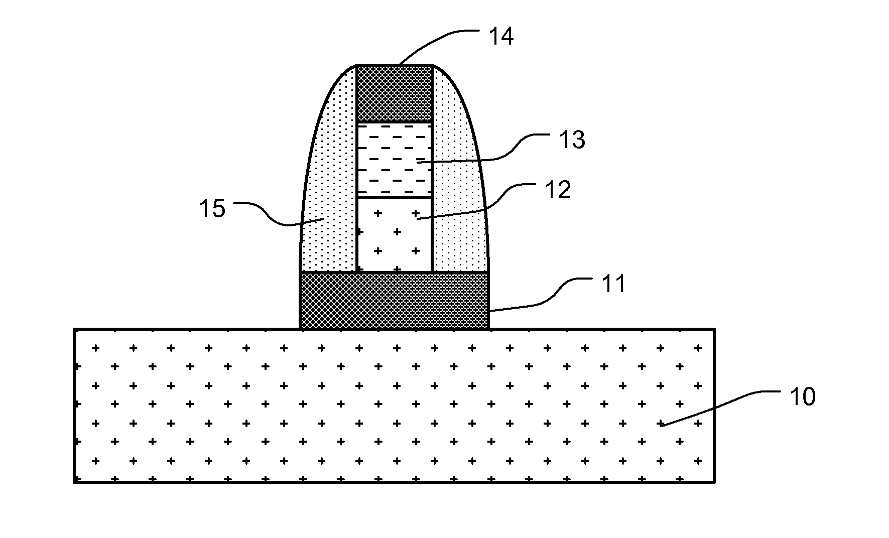
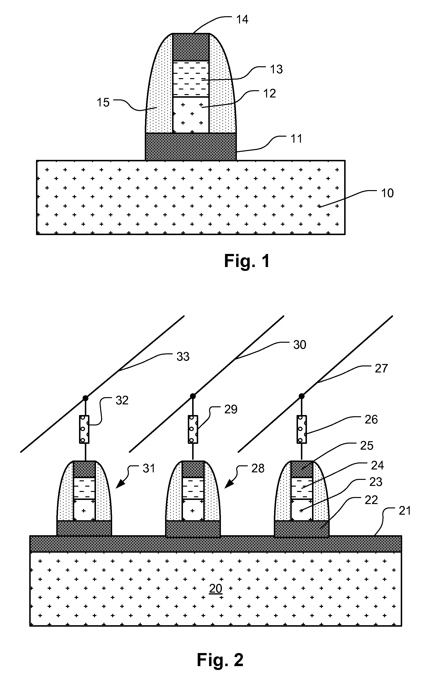
[0033]FIG. 1 illustrates an integrated circuit device formed on a single crystal silicon body 10, such as an epitaxial silicon layer in a silicon-on-insulator structure or a bulk silicon substrate. The device includes a silicide element 11, on top of which is a single crystal silicon node 12. A second semiconductor node 13 having a conductivity type opposite that of the single crystal silicon node 12 contacts the single crystal silicon node 12 forming a pn-junction therebetween. In the illustrated structure, a silicide cap 14 is formed on a second semiconductor node 13. Sidewall structures 15 isolate the pn-junction device from surrounding structures not shown. In the example of FIG. 1, a diode is shown using a single crystal silicon node 12 as one of the anode and cathode of the device. The single crystal silicon node 12 can be utilized in a variety of other structures as well, including transistors, and as a substrate on which additional layers can be formed which benefit from the...
PUM
 Abstract
Description
Claims
Application Information
 - R&D
- Intellectual Property
- Life Sciences
- Materials
- Tech Scout
- Unparalleled Data Quality
- Higher Quality Content
- 60% Fewer Hallucinations
Browse by: Latest US Patents, China's latest patents, Technical Efficacy Thesaurus, Application Domain, Technology Topic, Popular Technical Reports.
© 2025 PatSnap. All rights reserved.Legal|Privacy policy|Modern Slavery Act Transparency Statement|Sitemap|About US| Contact US: help@patsnap.com