Semiconductor device and manufacturing method thereof
a technology of semiconductor devices and semiconductors, applied in semiconductor devices, semiconductor/solid-state device details, electrical apparatus, etc., can solve the problems of reducing production yield, difficult to use flexible substrates made of plastics or something with a low melting point, and crystalline silicon application complicates the fabrication process, so as to reduce contact resistance
- Summary
- Abstract
- Description
- Claims
- Application Information
AI Technical Summary
Benefits of technology
Problems solved by technology
Method used
Image
Examples
exemplary embodiment 1
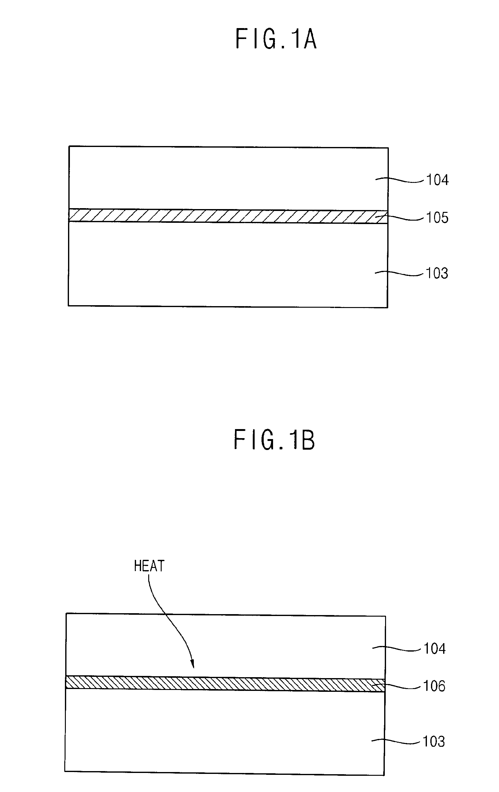
[0027]FIG. 1A shows a contact layer 105 placed between a semiconductor layer 103 and a wiring 104. In this exemplary embodiment of the invention, a low resistant contact layer 106 (depicted in FIG. 1B) is formed, which may improve the crystallinity of the semiconductor layer 103.
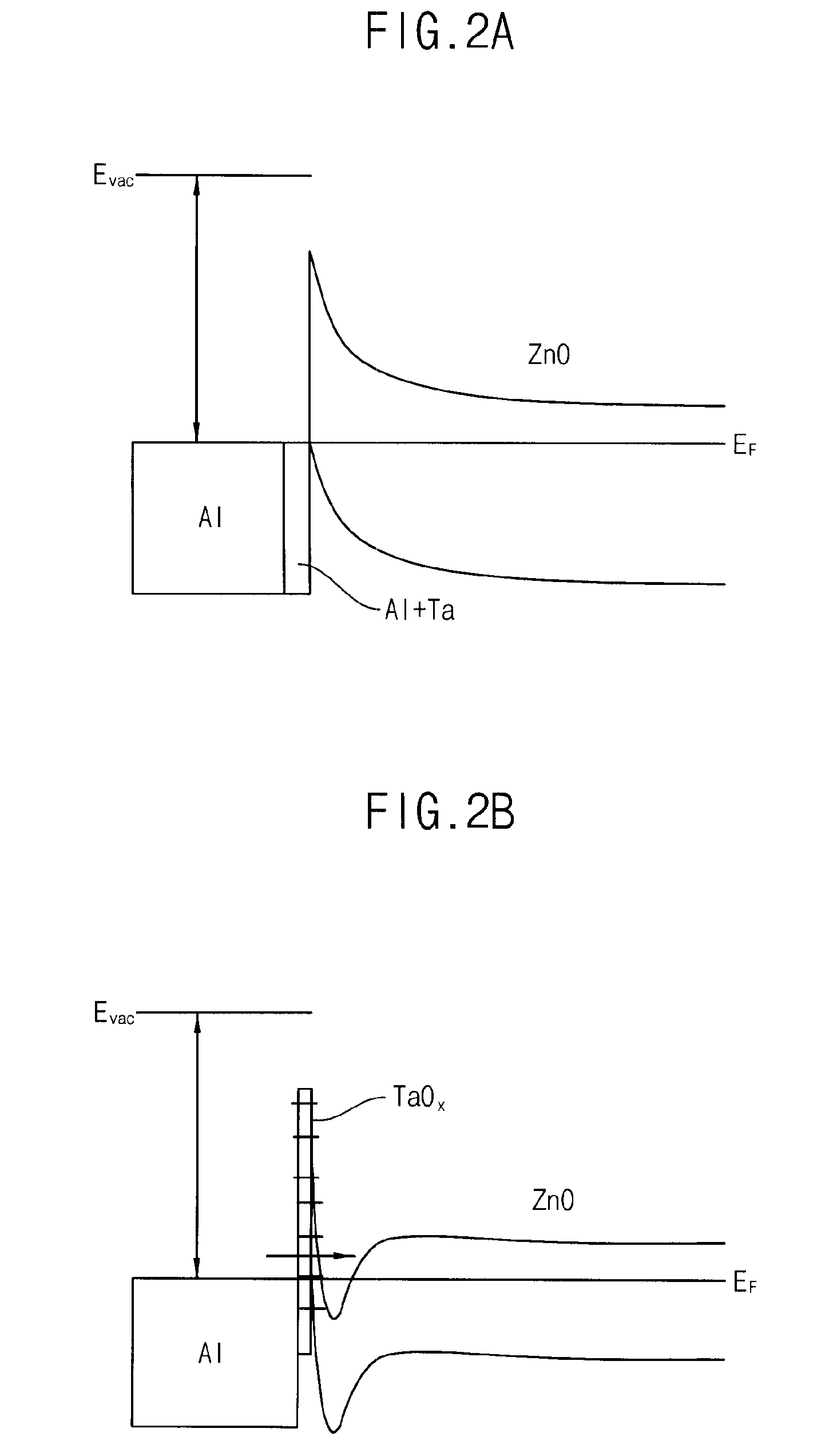
[0028]The semiconductor layer 103 in one exemplary embodiment of the invention is highly doped. For example, semiconductor layer 103 may include n+Si on amorphous Si, which may overcome a Schottky barrier to provide a low resistant contact layer between semiconductor layer 103 and wiring 104. This example utilizes the physical principle that contact resistance depends particularly on doping concentration, as described in Equation 1 below.
Rc=Aexp[(2ΦBn(N / m*∈s)1 / 2) / {coth(q / 2kT(N / m*∈s)1 / 2)}] (1)
[0029]Rc is the contact resistance, N is the doping concentration, ΦBn is the barrier height in an energy band diagram, and T is temperature.
[0030]However, a highly doped oxide semiconductor layer may not be a low resis...
exemplary embodiment 2
[0037]In this exemplary embodiment of the invention, a nitride semiconductor layer 103 including a low resistant contact layer 106 is formed and crystallinity may be improved. Exemplary Embodiment 2 is similar to Exemplary Embodiment 1 except for the semiconductor layer 103.
[0038]The present exemplary embodiment provides a method for producing a highly conductive non-stoichiometric nitride interlayer 106 between the nitride semiconductor layer 103 and the wiring 104 to lower the barrier height, ΦBn in Equation 1.
[0039]The nitride semiconductor layer 103 may include gallium nitride (GaN) in an amorphous state, a polycrystalline state, or a microcrystalline state in which both amorphous and polycrystalline states exist, and one or more impurity elements selected from a Group 1 element (for example, lithium (Li), sodium (Na), kalium (K), rubidium (Rb), or cesium (Cs)), a Group 13 element (for example, boron (B), gallium (Ga), indium (In), or thallium (Ti)), a Group 14 element (for exam...
exemplary embodiment 3
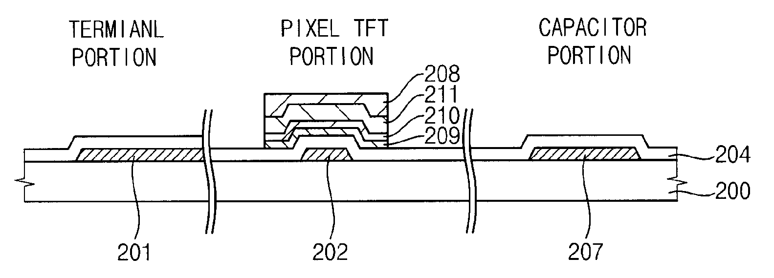
[0044]A semiconductor device including a field effective thin layer transistor is shown in the following exemplary embodiment. The steps in a process of manufacturing the device are shown in FIG. 3A, FIG. 3B, FIG. 3C, FIG. 3D, FIG. 3E, FIG. 3F, FIG. 3G, and FIG. 3H.
[0045]Referring to FIG. 3A, a substrate 101 may include barium borosilicate glass, alumino borosilicate glass, or the like. Alternatively, the substrate 101 may be a plastic substrate or a resin substrate including polyethylene terephthalate (PET), polyethylene naphthalate (PEN), polyether sulfone (PES), acrylic, polyimide, or the like.
[0046]A base layer 102 is formed on the substrate 101. The base layer 102 may be an insulating layer, such as a silicon oxide layer, a silicon nitride layer, a silicon oxynitride layer, or stacked layers thereof. The base layer 102 may be formed by a sputtering method or a CVD method. Note that the base layer 102 may be omitted.
[0047]Referring to FIG. 3B, an oxide semiconductor layer 103 ma...
PUM
 Abstract
Description
Claims
Application Information
 - R&D
- Intellectual Property
- Life Sciences
- Materials
- Tech Scout
- Unparalleled Data Quality
- Higher Quality Content
- 60% Fewer Hallucinations
Browse by: Latest US Patents, China's latest patents, Technical Efficacy Thesaurus, Application Domain, Technology Topic, Popular Technical Reports.
© 2025 PatSnap. All rights reserved.Legal|Privacy policy|Modern Slavery Act Transparency Statement|Sitemap|About US| Contact US: help@patsnap.com


