Substrate processing method

Inactive Publication Date: 2009-08-20
TOKYO ELECTRON LTD
View PDF6 Cites 1 Cited by
  • Summary
  • Abstract
  • Description
  • Claims
  • Application Information

AI Technical Summary

Benefits of technology

[0007]The present invention provides a substrate processing method that can prevent a decrease in the yield of semiconductor devices manufactured from substrates.
[0009]According to the present invention, the gas containing fluorine atoms is supplied into the processing container, the chlorine gas is supplied into the processing container, and further, the gas containing nitrogen atoms is supplied into the processing container. If the gas containing fluorine atoms is supplied in the case that water remains on the substrate, hydrogen fluoride is produced on the substrate, but after that, because the chlorine gas is supplied, the hydrogen fluoride reacts with the chlorine gas and turns into hydrogen chloride. Because the boiling point of the hydrogen chloride is considerably lower than the boiling point of the hydrogen fluoride so that the hydrogen chloride immediately vaporizes, the hydrogen chloride can be easily removed from the substrate. Moreover, even if water remains on the substrate when the hydrogen fluoride is produced, the water reacts with the chlorine gas and turns into hydrogen chloride, and hence the water can be easily removed from the substrate. That is, in the case that water remains on the substrate, even if a gas containing fluorine atoms is supplied toward the substrate, and hydrogen fluoride is produced, the hydrogen fluoride is converted into hydrogen chloride and easily removed from the substrate, and hence foreign matter can be simply and easily prevented from being produced on the substrate due to a chemical reaction of hydrogen fluoride and the gas containing nitrogen atoms. Similarly, water remaining on the substrate when the hydrogen fluoride is produced is also converted into hydrogen chloride, and hence foreign matter can be simply and easily prevented from being produced on the substrate due to the presence of water. Moreover, because there is no need to irradiate vacuum ultraviolet light to the substrate in order to remove fluorine, deterioration of a photoresist film on the substrate can be prevented. As a result, a decrease in the yield of the semiconductor devices manufactured from the substrates can be prevented.
[0011]According to the present invention, the temperature of the substrate is maintained at 20° C. or higher when the chlorine gas is supplied. The boiling point of hydrogen fluoride is approximately 19.5° C. at atmospheric pressure, and the temperature of the substrate when the chlorine gas is supplied is higher than the boiling point of hydrogen fluoride, and hence even if, when the chlorine gas is supplied, hydrogen fluoride that has not reacted with the supplied chlorine gas remains, the hydrogen fluoride that has not reacted with the supplied chlorine gas can be reliably vaporized. As a result, a decrease in the yield of the semiconductor devices manufactured from the substrates can be reliably prevented.
[0013]According to the present invention, the substrate is heated to 200° C. or higher when the chlorine gas is supplied. The temperature of the substrate when the chlorine gas is supplied is sufficiently higher than the boiling point of hydrogen fluoride, and hence even if, when the chlorine gas is supplied, hydrogen fluoride that has not reacted with the supplied chlorine gas remains, the hydrogen fluoride that has not reacted with the supplied chlorine gas can be more reliably vaporized. As a result, a decrease in the yield of the semiconductor devices manufactured from the substrates can be more reliably prevented.
[0017]According to the present invention, because plasma is not used in the chlorine supplying step, unwanted damage to the substrate can be prevented.

Problems solved by technology

If such reaction product remains as foreign matter on the wafer, short-circuiting of wiring occurs in a product manufactured from the wafer, for example, a semiconductor device, resulting in the yield of semiconductor devices decreasing.
In particular, water and fluorine atoms may cause foreign matter to be produced on the surface of the wafer with high probability.
However, in the above described method in which vacuum ultraviolet light is irradiated, equipment for irradiating vacuum ultraviolet light is required, and on the other hand, water on a wafer cannot be positively removed.
It is thus difficult to easily and reliably prevent foreign matter from being produced on a wafer.
Moreover, a photoresist film formed on a wafer deteriorates due to the irradiation of vacuum ultraviolet light to the wafer.
Thus, there is the problem that semiconductor devices are manufactured from a wafer on the surface of which foreign matter remains, a wafer whose photoresist film has deteriorated, and so on, resulting in the yield of the semiconductor devices ultimately manufactured decreasing.

Method used


Image

  • Substrate processing method
  • Substrate processing method
  • Substrate processing method

Examples


example 1

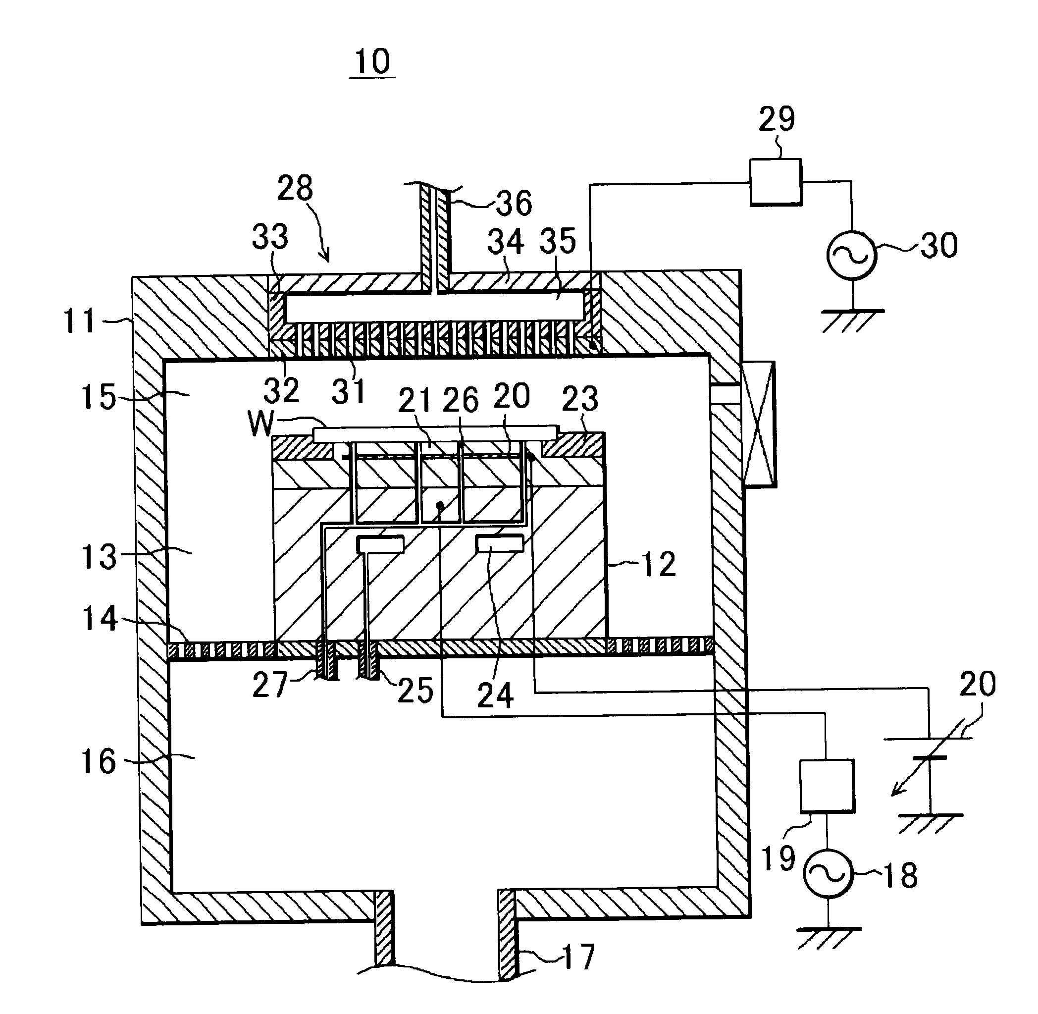
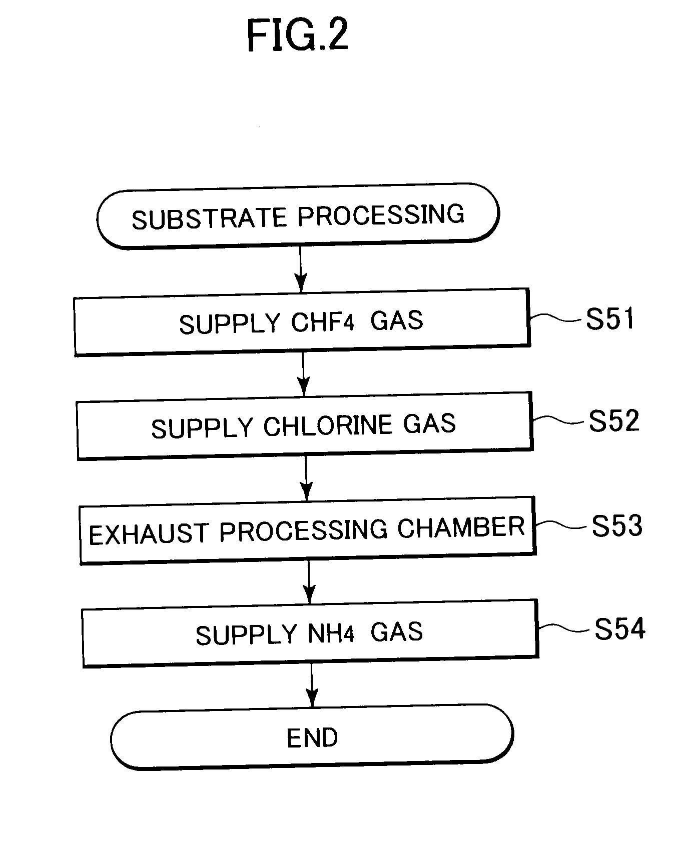
[0053]First, in the substrate processing apparatus 10, a process gas containing carbon tetrafluoride gas was supplied into the reaction chamber 15 in which a wafer W was accommodated. After that, the pressure in the reaction chamber 15 was reduced to a vacuum state, and radio frequency electrical power was supplied, whereby the process gas was turned into plasma. A polysilicon layer on the wafer W was subjected to the plasma etching using the plasma. Next, the pressure in the reaction chamber 15 was increased to atmospheric pressure, and a sufficient amount of chlorine gas was supplied into the reaction chamber 15. After that, the gas in the reaction chamber 15 is exhausted via the exhaust pipe 17. Subsequently, ammonia gas was supplied into the reaction chamber 15, and the wafer W was cleaned using the ammonia gas and then taken out from the chamber 11. Then, the surface of the wafer W was observed using a microscope, and it was ascertained that there was no foreign matter on the s...

example 2

[0057]First, at atmospheric pressure, a single gas comprised of hydrogen fluoride gas was supplied to a wafer W that had been subjected to the plasma etching. Then, the wafer W was heated to a temperature of 200° C., and a mixed gas comprised of hydrogen fluoride gas and nitrogen gas was supplied to the wafer W. Next, chlorine gas was supplied toward the wafer W, and then ammonia gas was supplied toward the wafer W. Then, the surface of the wafer W was observed using a microscope, and it was ascertained that there was no foreign matter on the surface of the wafer W.


PUM


Abstract

A substrate processing method that can prevent a decrease in the yield of semiconductor devices manufactured from substrates. A gas containing fluorine atoms is supplied into a chamber, and then chlorine gas is supplied into the chamber. Further, a gas containing nitrogen atoms is supplied into the chamber.

Description

BACKGROUND OF THE INVENTION[0001]1. Field of the Invention[0002]The present invention relates to a substrate processing method, and in particular relates to a substrate processing method in which a substrate is subjected to processing using a gas containing fluorine atoms and a gas containing nitrogen atoms.[0003]2. Description of the Related Art[0004]In the case that in a processing container, a wafer for a semiconductor device (hereinafter referred to merely as a “wafer”) as a substrate is subjected to desired processing using a process gas, the process gas and water existing in the processing container react with a surface of the wafer e.g. silicon (Si), and as a result, reaction product is produced. If such reaction product remains as foreign matter on the wafer, short-circuiting of wiring occurs in a product manufactured from the wafer, for example, a semiconductor device, resulting in the yield of semiconductor devices decreasing.[0005]In particular, water and fluorine atoms m...

Claims


Application Information

Patent Timeline
IPC IPC(8): H01L21/3065H01L21/306
CPCH01L21/02068
Inventor MORIYA, TSUYOSHINISHIMURA, EIICHI
Owner TOKYO ELECTRON LTD
Why Eureka
Try Eureka