
Sub-lithographic faceting for mosfet performance enhancement

a technology of mosfet and performance enhancement, which is applied in the field of semiconductor semiconductor (cmos) transistors, can solve the problems of high defect density near the boundary, adversely affect the performance of mosfet, and complex process complexity, and achieve the effect of less stringent alignment requirements

Inactive Publication Date: 2008-07-17
GLOBALFOUNDRIES INC
View PDF21 Cites 9 Cited by
  • Summary
  • Abstract
  • Description
  • Claims
  • Application Information

AI Technical Summary

Benefits of technology

[0012]The present invention limits the vertical variation of profiles of V-shaped grooves to less than about ⅓ of the minimum lithographic dimension, “F,” through the use of sub-lithographic self-assembly of resist material to address the need for facets with limited variation in the vertical profile of the V-shaped structure.
[0022]According the second embodiment of the present invention, after the anisotropic etch forms multiple non-adjoining parallel V-shaped grooves between the parallel lines of the self-aligned self-assembling material, a sacrificial oxide is formed on the multiple non-adjoining parallel V-shaped grooves with crystallographic facets by growth or deposition. Next, the volume above the sacrificial oxide between the multiple stacks of remaining pad oxide and pad nitride of sub-lithographic widths is filled with a second photoresist. Preferably, the filling of the volume between the stacks of sub-lithographic widths is achieved by applying the second photoresist and recessing it such that no resist remains on the wafer except between the stacks of sub-lithographic widths. Preferably, the NFET area of the silicon substrate is masked with a third photoresist to protect the pad oxide and pad nitride in the NFET area.
[0027]Another aspect of the present invention is that the self-aligned self-assembling material forms multiple parallel lines of sub-lithographic widths. The benefits of this feature include the increase in the channel area by a factor of the inverse of the cosine of the angle of the facets to the original flat surface of the substrate, the increased minority carrier mobility achieved by the use of optimal crystallographic facets for the formation of the channel, and the minimized variation in the height of the semiconductor surfaces upon which MOSFET devices are built.
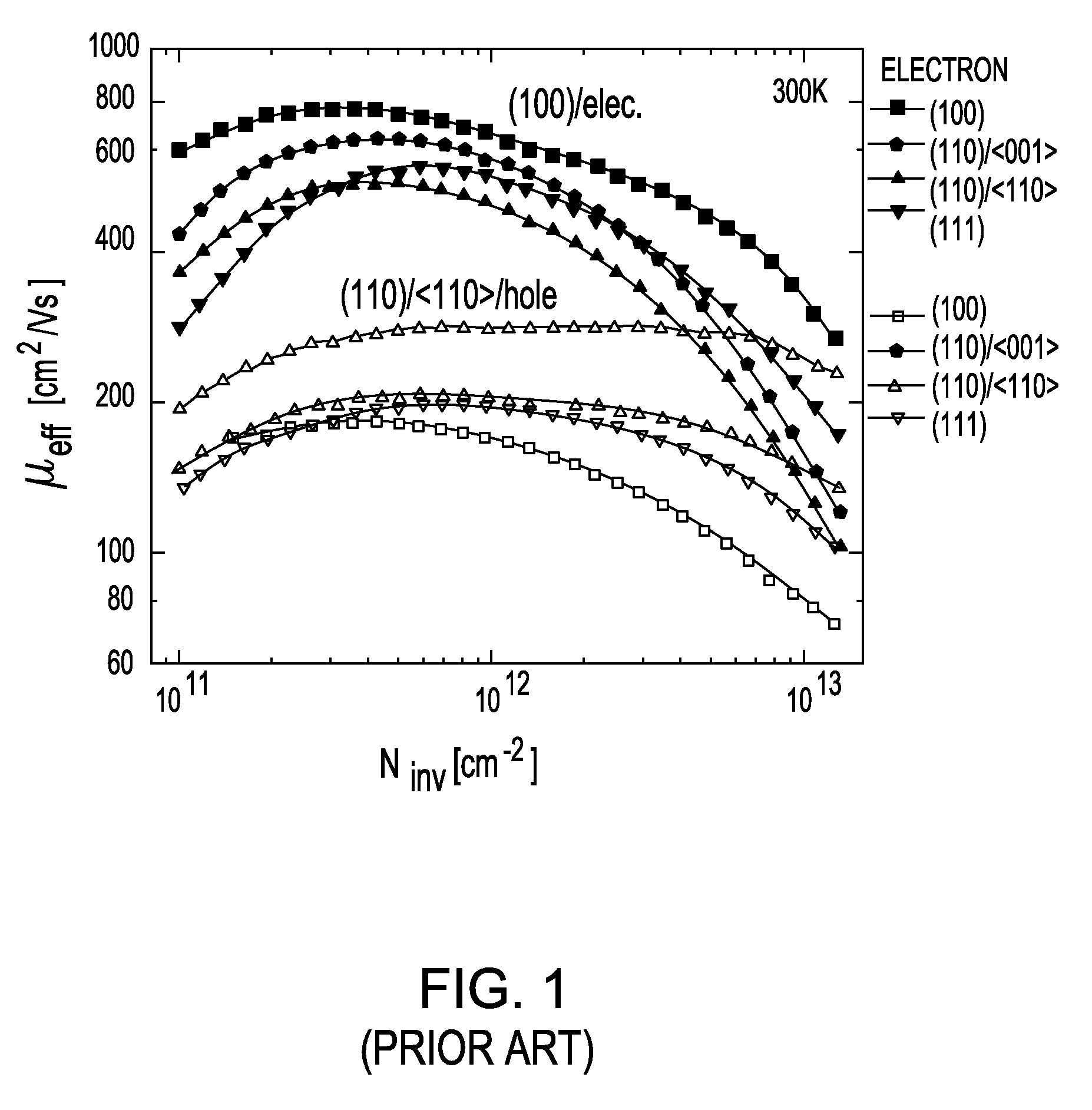
[0030]Both embodiments enable PFETs built on {110} facets formed on the V-shaped grooves and NFETs built on surfaces with the substrate orientation of (100). This enables the maximum mobility for both the PFETs and the NFETs
[0035]The present invention can also be practiced with the self-alignment of the V-shaped grooves to the STI. This is because the STI can serve as a natural limit for the formation of one of the two parallel edges for the V-shaped grooved formed adjacent to it. Even if the size of the facet that is adjacent to the STI is different from the size of the facets not adjoining the STI, the performance of the MOSFET formed on the multiple parallel V-shaped grooves is not affected significantly. However, the mask used for the patterning of the first photoresist may be advantageously allowed to have less stringent requirement for alignment, for example, by requiring a mid-ultraviolet (MUV) mask instead of a deep-ultraviolet (DUV) mask.

Problems solved by technology

General disadvantages of this type of approach include defect generation during the epitaxial growth of the semiconductor, a high level of defect density near the boundaries, and the complexity and cost of the processes.
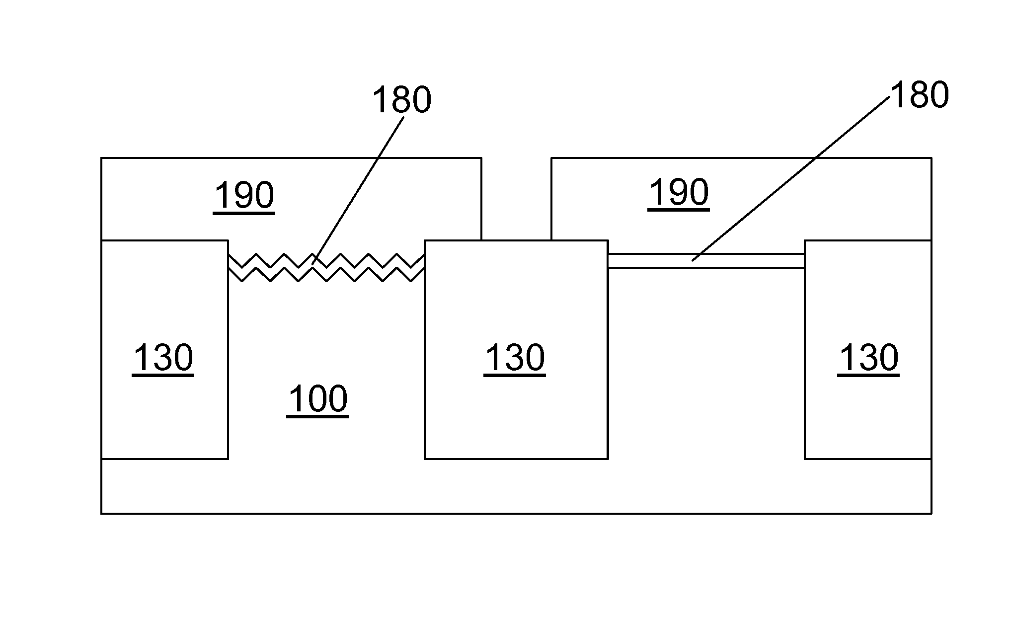
Formation of crystallographic facets, such as may be formed by V-shaped grooves, is subject to some limitations that adversely affect the performance of a MOSFET.
Also, in the cases involving an SOI substrate, a V-shaped groove wider than about twice the thickness of the semiconductor material above the buried oxide (BOX) layer becomes impossible since an attempt at generation of a V-shaped groove would expose the BOX layer before a wide V-shaped groove can be formed due to the limited thickness of the semiconductor layer above the BOX layer.
Limiting the width of the devices built on V-shaped grooves below a limit placed either due to the field of depth requirement of subsequent lithography steps or due to a limited thickness of the top semiconductor layer of an SOI substrate severely limits the layout of the MOSFET design utilizing V-shaped grooves.
This deteriorates the I_on to I_off ratio of the device.

Method used


Image

  • Sub-lithographic faceting for mosfet performance enhancement
  • Sub-lithographic faceting for mosfet performance enhancement
  • Sub-lithographic faceting for mosfet performance enhancement

Examples


first embodiment

[0059]According to the present invention, a first photoresist 135 is applied to the top surface of the silicon substrate patterned with STI 130. The first photoresist is patterned to create a space with parallel edges over the PFET area. The parallel edges of the first photoresist are preferably located outside the PFET area within the adjoining STI 130. Thereafter, a self-aligning self-assembling material is applied to the space over the PFET area and allowed to self-assemble and self-align to the surrounding pattern of the first resist 136. The self-aligned self-assembled resist 136 creates a pattern of multiple parallel lines as shown in FIG. 8A-8B within the space formed over the PFET area. Multiple parallel lines of the underlying pad nitride 120 are also exposed underneath the spaces between the pattern of multiple parallel lines formed by the self-aligned self-assembling material 136.

[0060]The exposed pattern, that is, the multiple parallel lines, over the pad nitride 120 is ...

second embodiment

[0069]According to the present invention, the multiple stacks of remaining pad oxide 110′ and pad nitride 120′ of sub-lithographic widths are then removed to expose a second portion 103 of the silicon surface preferably with a RIE process as shown in FIGS. 19A-19B. The second portion 103 is the flat portion of silicon surface between the edges of neighboring pairs of the multiple parallel non-adjoining V-shaped grooves 102.

[0070]Preferably, the second photoresist 155 and the third resist 165 are also removed leaving only sacrificial oxide 144 over the non-adjoining parallel V-shaped grooves 102. The resulting structure has the sacrificial oxide 144 over the multiple parallel non-adjoining V-shaped grooves 102 separated by a second portion103 between the edges of neighboring pairs of the multiple parallel non-adjoining V-shaped grooves 102 as shown in FIGS. 20A-20B.

[0071]A second anisotropic etch is then performed to form a second set of multiple parallel V-shaped grooves between the...


PUM


Abstract

The present invention provides structures and methods for providing multiple parallel V-shaped faceted grooves with sub-lithographic widths on a semiconductor substrate for enhanced performance MOSFETs. A self-aligning self-assembling material is used to pattern multiple parallel sub-lithographic lines. By employing an anisotropic etch that produces crystallographic facets on a semiconductor surface, multiple adjoining parallel V-shaped grooves with sub-lithographic groove widths are formed. While providing enhanced mobility for the MOSFET, the width of the MOSFET is not limited by the depth of focus in subsequent lithographic steps or the thickness of semiconductor layer above a BOX layer due to the sub-lithographic widths of the V-shaped grooves and the consequent reduction in the variation of the vertical profile. Also, the MOSFET has a well defined threshold voltage due to the narrow widths of each facet.

Description

FIELD OF THE INVENTION[0001]The present invention relates to semiconductor devices, and particularly, to complementary metal oxide semiconductor (CMOS) transistors having facets with sub-lithographic widths.BACKGROUND OF THE INVENTION[0002]Performance of semiconductor field effect transistors depends on the crystallographic surface orientation on which the channel of the transistor is built through the mobility of minority channel carriers. For example, the electron mobility in silicon is the highest for the {100} surface orientations and the lowest for the {110} surface orientations, while the hole mobility is the highest for the {110} surface orientations and the lowest for the {100} surface orientations within silicon single crystal.[0003]Use of different crystallographic planes for PFET and NFET devices to enhance the performance of the overall circuit has been known in the prior art. This class of technology, called “hybrid orientation technology (HOT)” in the industry, provide...

Claims


Application Information

Patent Timeline
Patent Type & Authority Applications(United States)
IPC IPC(8): H01L29/06H01L21/311
CPCH01L21/28123H01L21/3086H01L21/3088H01L29/78H01L29/0673H01L29/1037H01L21/823807
Inventor BUTT, SHAHID A.DYER, THOMAS W.KWON, OH-JUNGMANDELMAN, JACK A.YANG, HAINING S.
Owner GLOBALFOUNDRIES INC
Learn More