Semiconductor device and manufacturing method therof

a technology of semiconductor devices and manufacturing methods, applied in semiconductor devices, semiconductor/solid-state device details, electrical apparatus, etc., can solve problems such as the increase of resistance between plugs and wires, and achieve the effect of reducing resistance values

Inactive Publication Date: 2007-06-28
PANASONIC CORP +1
View PDF2 Cites 53 Cited by
  • Summary
  • Abstract
  • Description
  • Claims
  • Application Information

AI Technical Summary

Benefits of technology

[0018]FIG. 8 shows a mechanism which is considered to be a cause of the increased resistance between the wire and the plug in the conventional method. In the conventional manufacturing method, heating after the formation of the first wire distributes Al included in the seed film 104 in the copper film 105, which forms a CuAl alloy. Especially, it is considered that after the via hole 108 is formed, the Al included in the seed film 104 bonds with atmospheric oxygen, so that not only a Cu oxide but also an Al oxide are formed on upper surface of the copper film 105 and on upper end surfaces of the seed film 104. The Al oxide can not be reduced in an annealing process in the hydrogen atmosphere performed before the formation of the barrier metal film 110, because the Al oxide has the intermolecular bond energy significantly stronger than that of the Cu oxide. For this reason, it can be considered that an Al oxide film 113 formed on the first wire can not be removed, so that the resistance value between the wire and the plug increases.
[0019] An object of the invention is to provide a semiconductor device without the above-mentioned problems, the semiconductor device being manufactured with a good yield and having high reliability and another object of the invention is to provide a manufacturing method of such semiconductor device.
[0024] According to this method, the metal oxide film formed on the first wiring material film is removed, so that it is possible to reduce the resistance value between the plug and the wire more than the conventional method reduces it.
[0026] In the method described above, the oxide film of the metal is first removed from the first wiring material film, and then the barrier metal film is formed. This makes it possible to reduce the resistance value between the plug and the wire more than the conventional method reduces it.

Problems solved by technology

However, the structure of the above-mentioned conventional semiconductor device and the manufacturing method have a problem that the resistance value between a plug and a wire may increase.

Method used


Image

  • Semiconductor device and manufacturing method therof
  • Semiconductor device and manufacturing method therof
  • Semiconductor device and manufacturing method therof

Examples


embodiment 1

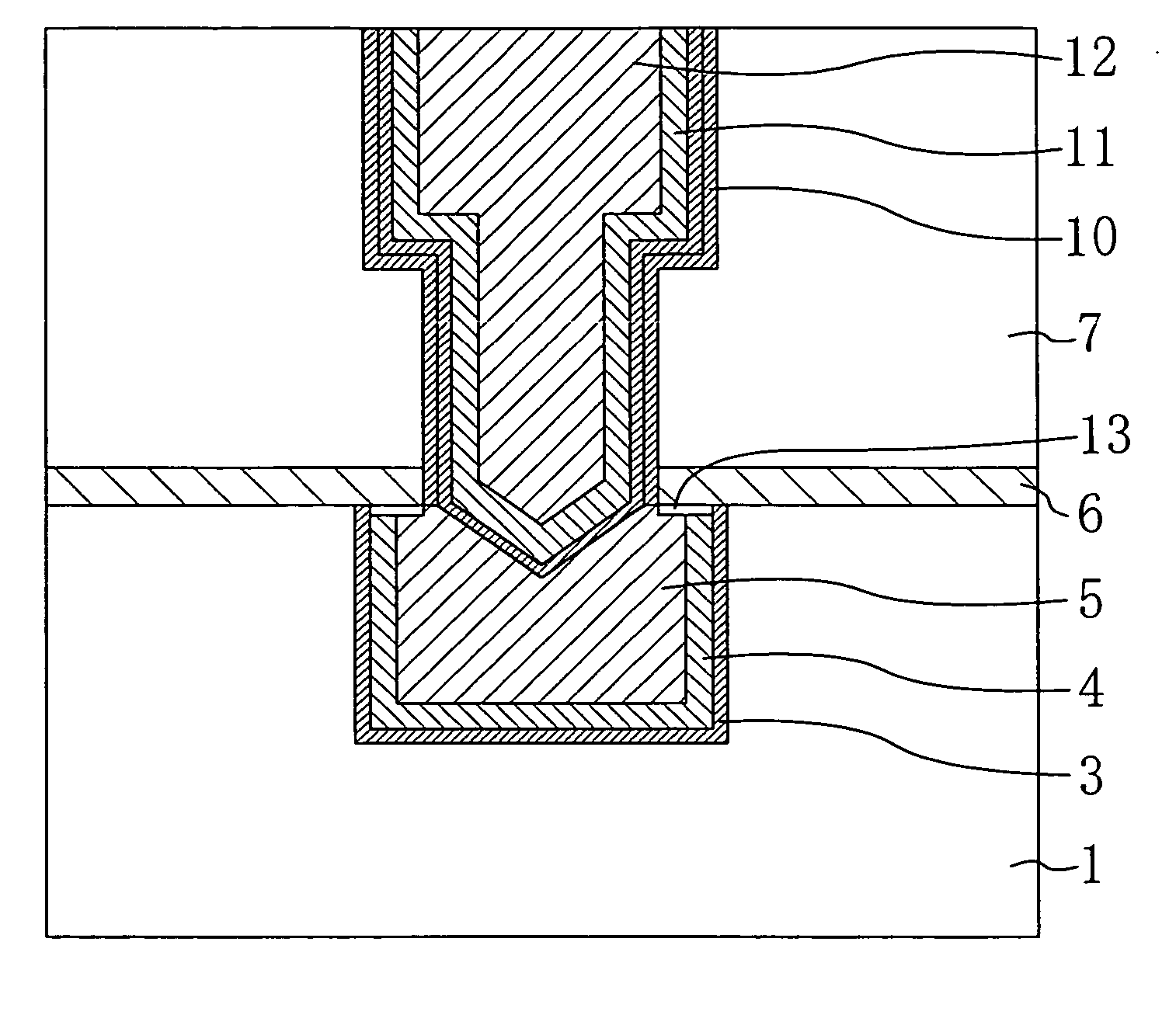
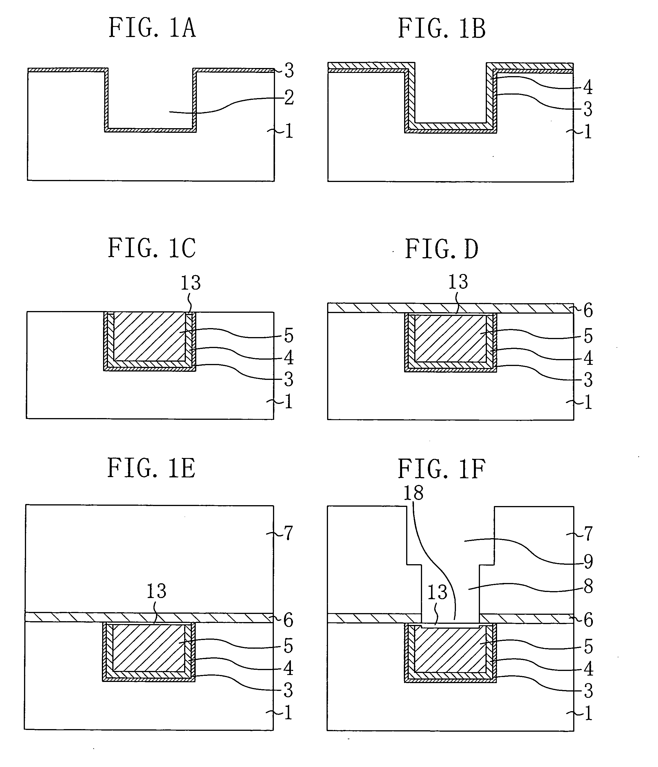
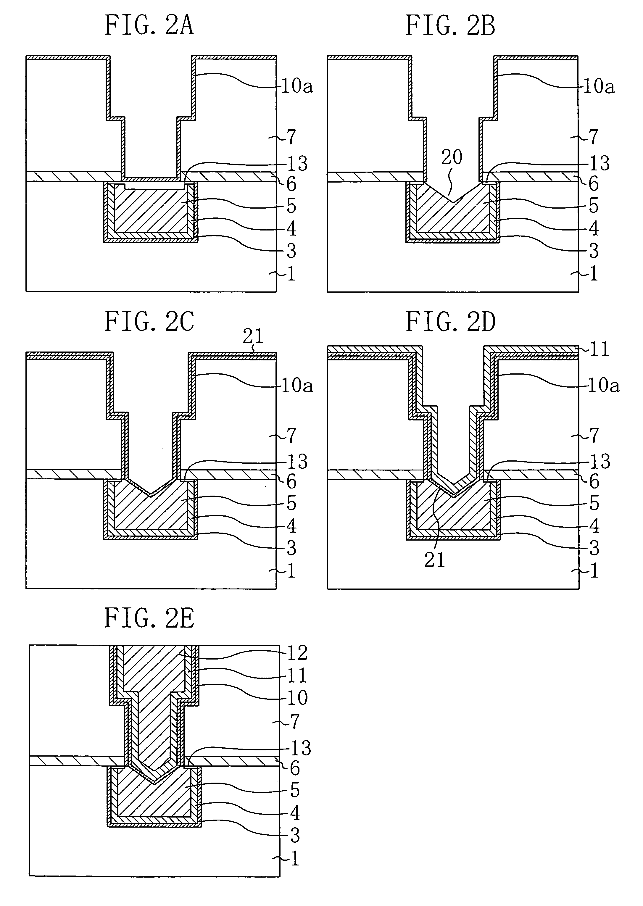
[0035]FIGS. 1A through 1F and FIGS. 2A through 2E are cross sections illustrating a semiconductor device manufacturing method according to Embodiment 1 of the present invention.

[0036] First, referring to FIG. 1A, a lithography step is performed to form a resist. Then, an etching process is performed using the resist as a mask so as to form a first wire trench 2 in a first interlayer dielectric film 1, the first interlayer dielectric film 1 being formed of a low dielectric constant material on a substrate (not shown). Next, as a preparatory process, an annealing process is performed on the substrate (semiconductor device) for 60 seconds in a hydrogen atmosphere at a temperature of 280° C. so as to reduce an oxide formed on a surface of the semiconductor device. Then, as a barrier metal film 3, a tantalum nitride film having a thickness of 5 nm and a tantalum film having a thickness of 10 nm are formed by, for example, sputtering. In this case, the barrier metal film 3 is a metal fil...

embodiment 2

[0055]FIGS. 4A through 4I are cross sections illustrating a semiconductor device manufacturing method according to Embodiment 2 of the present invention. The method of removing the Al oxide formed on the first wire in the manufacturing method of Embodiment 2 is different from that in the manufacturing method of Embodiment 1.

[0056] First, referring to FIG. 4A, a lithography step is performed to form a resist. Then, an etching process is performed using the resist as a mask so as to form a first wire trench 2 in a first interlayer dielectric film 1, the first interlayer dielectric film 1 being formed of a low dielectric constant material on a substrate (not shown). Next, as a preparatory process, an annealing process is performed on the substrate (semiconductor device) for 60 seconds in a hydrogen atmosphere at a temperature of 280° C. so as to reduce an oxide formed on a surface of the semiconductor device. Then, as a barrier metal film 3, a tantalum nitride film having a thickness ...


PUM


Abstract

The semiconductor device manufacturing method includes the steps of: applying a first wire including a barrier metal film, a seed film, and a wiring material film in a first wire trench formed in a first interlayer dielectric film; after a second interlayer dielectric film is formed on the first interlayer dielectric film, forming a via hole and a second wire trench in the second interlayer dielectric film so as to expose the wiring material film; applying a barrier metal film on the semiconductor device; and after the barrier metal film on the wiring material film is removed by using, for example, a re-sputtering process, applying a barrier metal film on the wiring material film. The re-sputtering process can remove an oxide film of impurity metal in the seed film applied on the wiring material film.

Description

BACKGROUND OF THE INVENTION [0001] 1. Field of the Invention [0002] The present invention relates to a semiconductor device having a structure of a metal wire provided in a trench and to a manufacturing method of the semiconductor device. [0003] 2. Description of the Related Art [0004] In recent years, due to progressing reduction of a wiring pitch in a device, it becomes increasingly important to ensure reliability of wiring. For this purpose, investigations have been made to improve the reliability by adding a variety of elements to copper used as a wiring material. [0005] A conventional semiconductor device having an embedded wire will be explained below. FIGS. 6A through 6I are cross sections illustrating a conventional manufacturing method of the semiconductor device. [0006] First, referring to FIG. 6A, a lithography step and an etching step are carried out to form a first wire trench 102 in a first interlayer dielectric film 101, the first interlayer dielectric film 101 being ...

Claims


Application Information

Patent Timeline
IPC IPC(8): H01L23/52
CPCH01L21/76805H01L21/76814H01L21/76843H01L21/76844H01L21/76856H01L21/76873H01L21/76886H01L2924/0002H01L23/5226H01L23/53238H01L23/53295H01L2924/00
Inventor YANO, HISASHIHAMADA, MASAKAZUMAEKAWA, KAZUYOSHIMORI, KENICHI
Owner PANASONIC CORP
Why Eureka
Try Eureka