Fabrication method of extreme ultraviolet radiation mask mirror using atomic force microscope lithography

Inactive Publication Date: 2007-03-08
IUCF HYU (IND UNIV COOP FOUNDATION HANYANG UNIV)
View PDF6 Cites 17 Cited by
  • Summary
  • Abstract
  • Description
  • Claims
  • Application Information

AI Technical Summary

Benefits of technology

[0033] In this manner, this invention uses a sputtering system for simultaneous deposition of a multi-layered thin film and an absorber layer reducing substrate contamination. A reduction in the surface roughness value which is an important factor in a lithographic process in obtaining minute patterns using an atomic force microscope is also obtained in this way.
[0038] During this process, a metal oxide product (9) equivalent to the one obtained in absence of resistant organic material is obtained when a resistant organic material (8) is coated on the absorber layer (7) during lithographic process as in FIG. 3, and this further increases the selectivity during an etching process.
[0044] A fine pattern down to a few nm wide as well as various pattern images can be obtained without any damage to a substrate using an atomic force microscope in the lithographic step of a semiconductor manufacturing process following the above-mentioned manufacturing process of this invention.

Problems solved by technology

Lasers are used as light sources, but traditional optical exposure processes have reached their limits in that they cannot be applied to manufacturing substrates with a minimum line width of less than 70 nm.
But, if an electron beam lithography such as the one mentioned above is used to pattern an absorbing layer, electron beam scattering causes damages to the substrate.
Minute patterns are also hard to achieve and the attainable line width is limited to around 30 nm.
But, this method can only be applied to absorbing materials that do not oxidize such as gold.

Method used


Image

  • Fabrication method of extreme ultraviolet radiation mask mirror using atomic force microscope lithography
  • Fabrication method of extreme ultraviolet radiation mask mirror using atomic force microscope lithography
  • Fabrication method of extreme ultraviolet radiation mask mirror using atomic force microscope lithography

Examples


Embodiment Construction

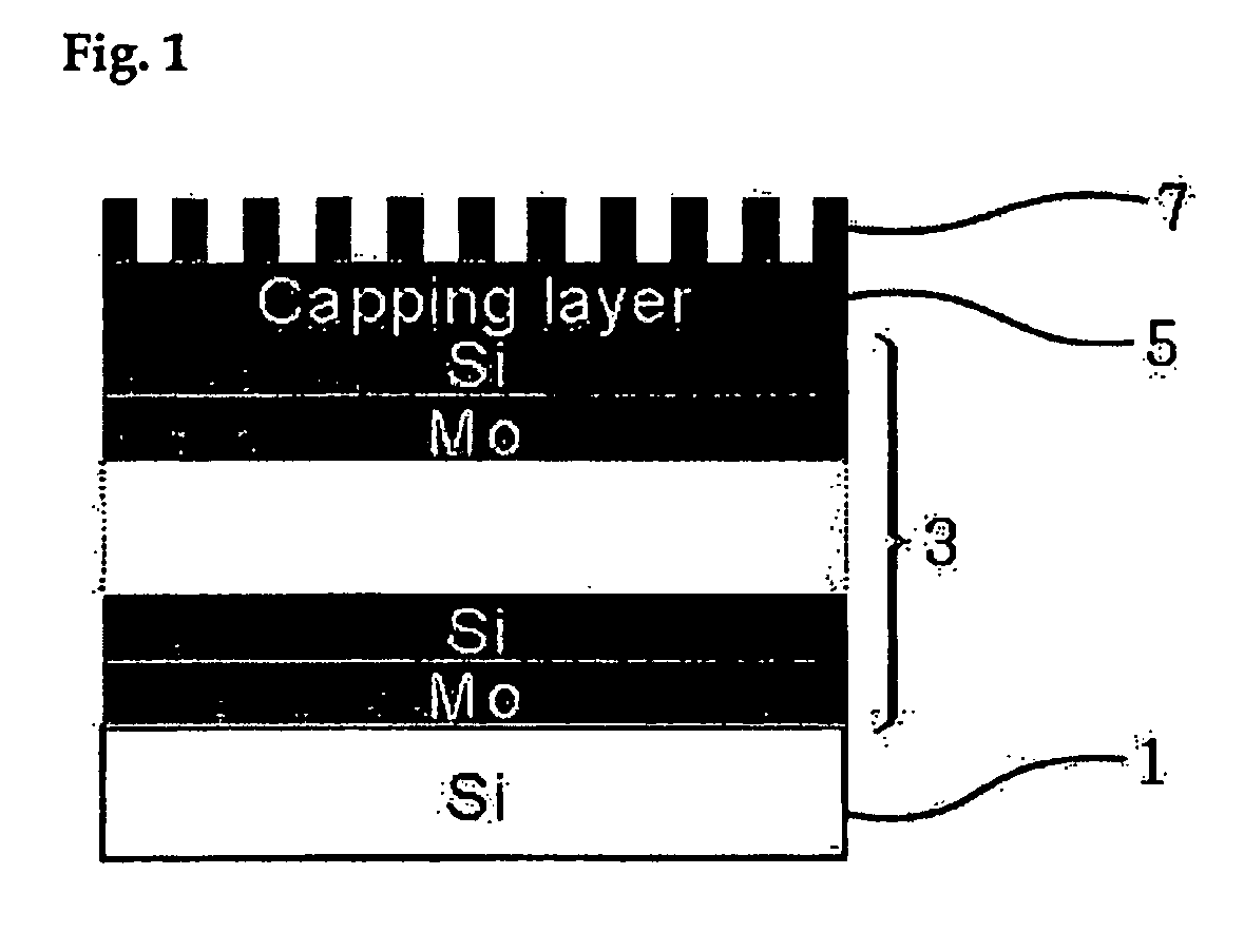
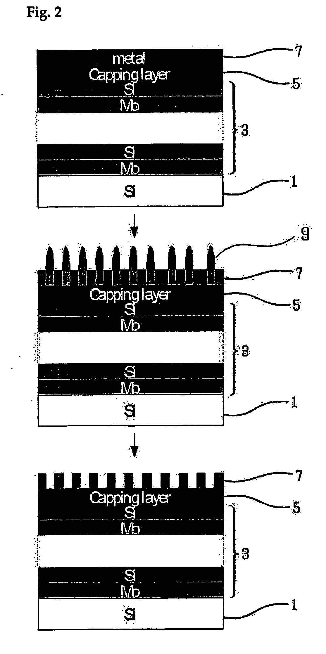
[0021] This invention relates to a method for manufacturing reflective multi-layered thin film mirrors for extreme ultraviolet radiation exposure processes, comprising: depositing reflective multi-layered thin film and protective layer on a silicon substrate; depositing a thin film of chromium, tantalum, or tungsten on this multi-layered thin film and protective layer; generating an oxidized metal structure with fixed height and width on the substrate surface by impressing electric field between a cantilever tip and the above-mentioned multi-layer structured substrate using an atomic force microscope; and etching this metal oxide structure to obtain an ultra-fine line width absorber pattern.

[0022] The manufacturing process of this invention further comprises depositing thin organic film as a resistant material on a thin absorber metal film after the deposition of a thin absorber metal film, and cleaning off this thin organic layer after etching the metal oxide layer. In addition, t...


PUM


Abstract

The present invention relates to a method for manufacturing a reflective multi-layered thin film mirror for an extreme ultraviolet radiation (EUV) exposure process that is one of the next generation exposure process masks using an atomic force microscope (AFM). This reflective multi-layered thin film mirror for extreme ultraviolet radiation (EUV) exposure process allows metal oxide structures with fixed height and width to be obtained using anodic oxidization phenomenon between the cantilever tip of a atomic force microscope and an absorber material during the patterning of an absorber layer on a multi-layered thin film of a substrate, followed by forming the ultra-fine line width absorber patterns via etching of the metal oxide structure. Use of the manufacturing process of this invention is advantageous in manufacturing of extreme ultraviolet radiation exposure mask mirrors with high resolution and in manufacturing of reflective multi-layered thin film mirrors with minute absorber pattern sizes (less than 20 nm line width) compared to traditional manufacturing methods.

Description

BACKGROUND OF INVENTION [0001] 1. Field of Invention [0002] The present invention relates to a manufacturing method of a reflective multi-layered thin film mirror for extreme ultraviolet radiation exposure process using atomic force microscope lithography, by forming a metal oxide structure with fixed height and width on a substrate using the anodic oxidation phenomenon between the probe of an atomic force microscope and an absorber for patterning of an absorber material deposited on the multi-layered thin film substrate, wherein the metal oxidic layer is etched to obtain an ultra-fine line patterned absorber. [0003] 2. Description of Related Art [0004] In manufacturing semiconductor elements, the optical lithographic process is the core process in creating circuit patterns by refractive light on a substrate coated with a light sensing film sensitive to light. Lasers are used as light sources, but traditional optical exposure processes have reached their limits in that they cannot b...

Claims


Application Information

Patent Timeline
IPC IPC(8): G03F1/00G03F1/08G03F1/14H01L21/027G03F1/24G03F7/20
CPCB82Y10/00B82Y30/00G03F7/2049G03F1/08G03F1/24B82Y40/00H01L21/027
Inventor LEE, HAI WONLEE, SUN WOOAHN, JIN HOBAE, SUK JONG
Owner IUCF HYU (IND UNIV COOP FOUNDATION HANYANG UNIV)
Why Eureka
Try Eureka