Variable transconductance circuit
a transconductance circuit and variable technology, applied in differential amplifiers, amplifiers with semiconductor devices/discharge tubes, amplifiers, etc., can solve problems such as increased current consumption, low power supply voltage operation is therefore difficult, and problems in current consumption and on-board circuit area, so as to reduce the amount of current change required for varying gm, high gm, and low power consumption
- Summary
- Abstract
- Description
- Claims
- Application Information
AI Technical Summary
Benefits of technology
Problems solved by technology
Method used
Image
Examples
embodiment 1
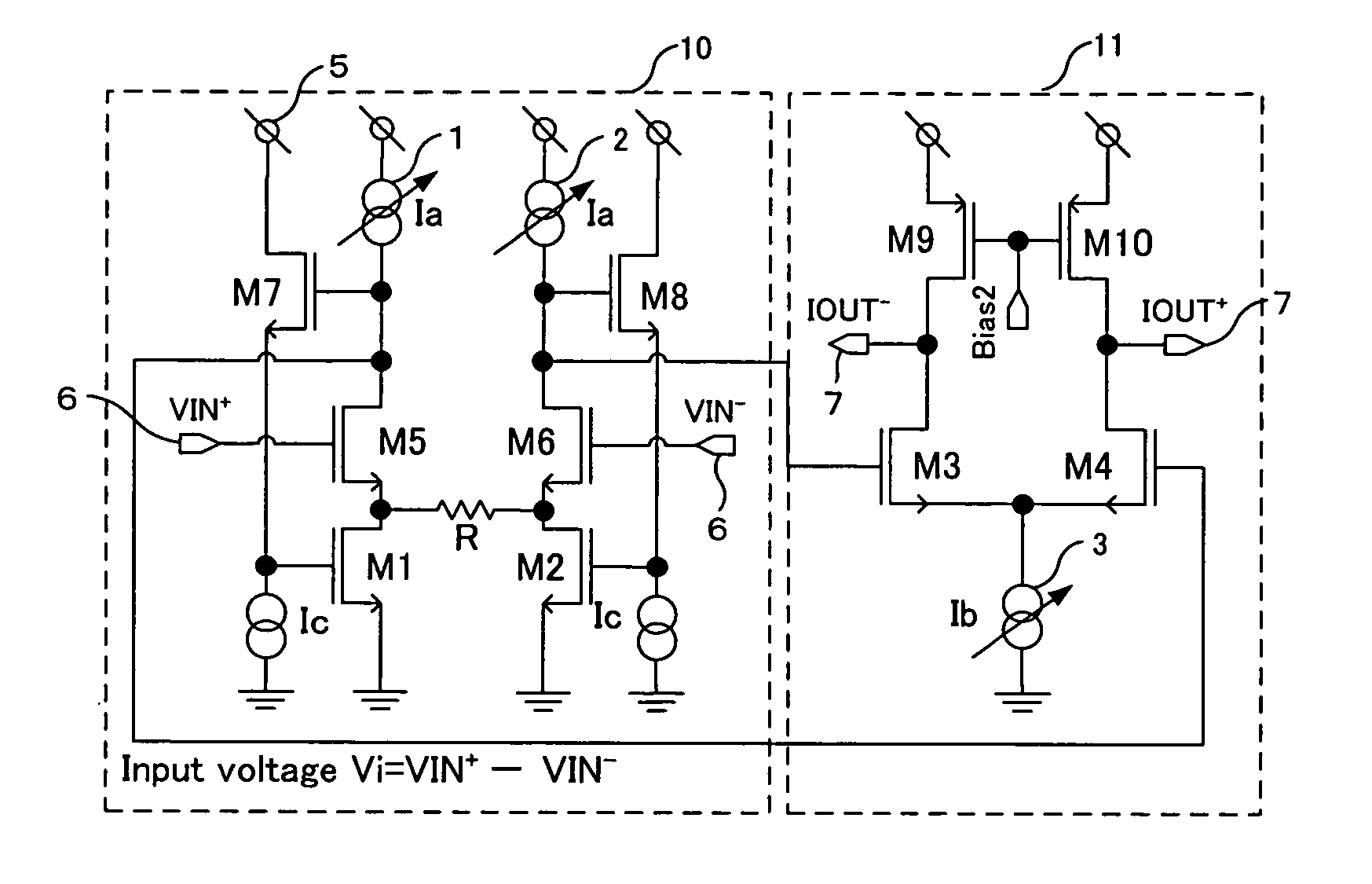
[0039]FIG. 1 shows a variable transconductance circuit of Embodiment 1. In a linear voltage current conversion section, which is configured as described in the prior art, an input voltage signal Vi is converted to a current with an inter-source resistance R between MOS transistors M5 and M6, to give a drain current for MOS transistors M1 and M2. At this time, the gate voltage difference between the MOS transistors M1 and M2 is represented by expression (4): Δ Vg=(la+ViRk 1·β-la-ViRk 1·β)(4)
where k1=gate width / gate length of MOS transistors M1 and M2 and β=charge mobility×capacity of gate oxide film / 2.
[0040] The gate voltages of the MOS transistors M1 and M2 are driven with the sources of MOS transistors M7 and M8 each constituting a source follower. If a substrate bias effect of the MOS transistors M7 and M8 is neglected, the above value ΔVg is equal to the gate voltage difference between the MOS transistors M7 and M8, that is, the drain voltage difference between the MOS t...
embodiment 2
[0043]FIG. 2 shows a variable transconductance circuit of Embodiment 2. In the variable transconductance circuit of FIG. 1, the gate voltages of the MOS transistors M4 and M3 are automatically determined with the gate-source voltages of the MOS transistors M1 and M7 and the MOS transistors M2 and M8, respectively. Therefore, to allow operation of the MOS transistors M3 and M4 in the saturation region, the output dynamic range is automatically determined, and this restricts the degree of design freedom. To solve this problem, in the variable transconductance circuit of FIG. 2, a level shift circuit 4 is interposed each between the gates of the MOS transistors M1 and M4 and between the gates of the MOS transistors M2 and M3. By appropriately setting the DC level shift amount of each of the level shift circuits 4, the degree of design freedom of the output dynamic range is improved. Alternatively, if the input impedance is sufficiently high, the level shift circuit 4 may be interposed ...
embodiment 3
[0044] In the configurations in FIGS. 1 and 2, the MOS transistors M1, M5 and M7 or the MOS transistors M2, M6 and M8 constitute a negative feedback loop. The unity gain frequency f0 of such a loop and Ia have the relationship of Expression (8) below, and thus the circuit frequency characteristic varies with gm.
f0∝√{square root over (Ia)} (8)
[0045]FIG. 3 shows a variable transconductance circuit of Embodiment 3 for solving the above problem. The MOS transistor M5 and a current source 1 constitute an output source follower for an operational amplifier, and the MOS transistor M6 and a current source 2 constitute another output source follower. The resistance R is connected between the outputs of the source followers. When the voltage signal Vi is input, the voltage difference of Vi also occurs at both ends of the resistance R, allowing flow of a signal current of Vi / R. This signal current, output from the drains of the MOS transistors M5 and M6, is input into the MOS transistors M1...
PUM
 Abstract
Description
Claims
Application Information
 - R&D
- Intellectual Property
- Life Sciences
- Materials
- Tech Scout
- Unparalleled Data Quality
- Higher Quality Content
- 60% Fewer Hallucinations
Browse by: Latest US Patents, China's latest patents, Technical Efficacy Thesaurus, Application Domain, Technology Topic, Popular Technical Reports.
© 2025 PatSnap. All rights reserved.Legal|Privacy policy|Modern Slavery Act Transparency Statement|Sitemap|About US| Contact US: help@patsnap.com


