
Method for forming fine copper particle sintered product type of electric conductor having fine shape, method for forming fine copper wiring and thin copper film using said method

Active Publication Date: 2006-09-21
HARIMA CHEM INC
View PDF3 Cites 41 Cited by
  • Summary
  • Abstract
  • Description
  • Claims
  • Application Information

AI Technical Summary

Benefits of technology

[0011] As explained above, the copper base wiring has such advantages that the material itself is inexpensive, and it may avoid the breaking of a wire due to electromigration or may alleviate a reduction / change in a thickness of a wiring layer even when applied to a high current density, so that an application of the copper base wiring to a conductor layer for a plated printed circuit having a fine wiring pattern is studied. In such a case, such a dispersion of copper fine particles with smaller particle diameters as to suite for drawing a fine pattern for wiring is required, and then because a surface oxide film layer covering the surface relatively increases with the decrease of the particle diameter, there is growing need for developing a technique for reducing the surface oxide film layer to produce a copper wiring layer of a sintered product type showing excellent electroconductivity. In addition, in the case of the copper fine particle with a finer average diameter, oxidation is advanced from the surface to the inside so as to convert the most parts of the particle into the copper oxides, and whereby it may turn into the particle equivalent to a fine particle made of copper oxides. Accordingly, as for such a copper oxide fine particle, in place of the copper fine particle having the surface oxide film layer, it becomes necessary to develop the technique for preparation of a copper wiring layer of a sintered product type showing good electroconductivity, through the process wherein the coating layer that is drown in the shape of fine pattern for wiring by using the dispersion thereof is subjected to rapid reduction at a low temperature to recover a cupper fine particle, and then said cupper fine particle is sintered with each other closely.
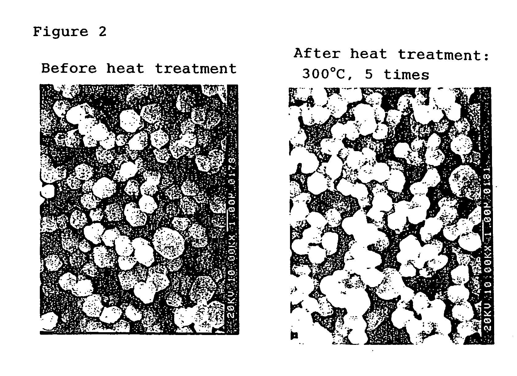
[0049] In the process for forming a fine copper-based wiring pattern as well as the process for a copper thin film according to the first aspect of the present invention described above, for a fine wiring pattern or a coating film pattern, which are drawn with the use of a dispersion containing copper nano-particles having an oxide film layer on its surface or copper oxide nano-particles which are in advanced stage of oxidation expanded into the whole particles, the nano-particles in a dispersion-coated layer are heated at 300° C. or lower in the presence of an organic compound having reducibility to reduce the oxide film covering thereon by means of the reduction reaction using the organic compound having reducibility as a reducing agent, and thereby the cupper nano-particles are recovered therefrom; as a result, formation of the product layer made of the resultant copper nano-particles sintered with each other can be achieved in the same heating step. The reduction of the copper oxide covering film layer by using the organic compound having reducibility as the reducing agent progresses at a sufficient reaction rate even at a low temperature of 300° C. or lower, and then the sintering of the recovered copper nano-particles with each other is as well executed coincidentally in the presence of said organic compound having reducibility, so that after the reduction treatment, re-oxidation of the active surface of the copper nano-particle can be avoided. The heat treatment can be performed at the low temperature of 300° C. or lower, so that heat resistance required to a substrate material to be used is greatly alleviated, which is an advantage in greatly widening a spectrum of application. In addition, with respect to the obtained fine copper-based wiring, as copper itself is a conductive material being low in the risk of electromigration, the occurrence of the decrease of a wiring thickness or the breaking of a wire due to the electromigration can be inhibited for the fine wiring patter described above. Furthermore, both of the used organic compound having reducibility and a reaction product which is by-produced from the organic compound in the reducing treatment are finally evaporated or gasified by heating, and as a result, there is a further advantage that they do not remain in the resultant fine copper-based wiring layer of a sintered product type or in the copper thin-film layer with an extremely thin film thickness.

Problems solved by technology

However, in contrast to gold and silver of noble metals, copper tends to be easily oxidized, and the continued progress of oxidation is made from its surface to its inside.
As a result, we could not find means for completely preventing the surface oxidation.
Hence, the dispersion of copper fine particles that employs the copper nano-particles and is applicable to reproducible preparation of a fine wiring pattern with the use of a sintered product type of wiring layer that is obtained by sintering the copper nano-particles with each other, and which can replace the technique of forming a ultra fine wiring pattern by using a uniform dispersion containing the nano-particles of gold and silver of noble metals, has not yet reached practical levels under present circumstances.
Accordingly, formation of a dense pass for current flow is not achieved within the sintered product wholly, so that it was hard to prepare a fine wiring pattern having desired good electroconductivity in high reproducibility with the use thereof.
Such a substrate material as to endure said treatment temperature is limited to some heat-resistant materials such as ceramic, and particularly the unnecessary reaction by-product will be left in the sintered product.
Therefore, there is no possibility that such a technique using the dispersion, in which the hydrogenating agent such as a boron hydride derivative is blended, will be widely applied.

Method used


Image

  • Method for forming fine copper particle sintered product type of electric conductor having fine shape, method for forming fine copper wiring and thin copper film using said method
  • Method for forming fine copper particle sintered product type of electric conductor having fine shape, method for forming fine copper wiring and thin copper film using said method
  • Method for forming fine copper particle sintered product type of electric conductor having fine shape, method for forming fine copper wiring and thin copper film using said method

Examples


examples 1-1 to 1-4

AND COMPARATIVE EXAMPLES 1-1 TO 1-3

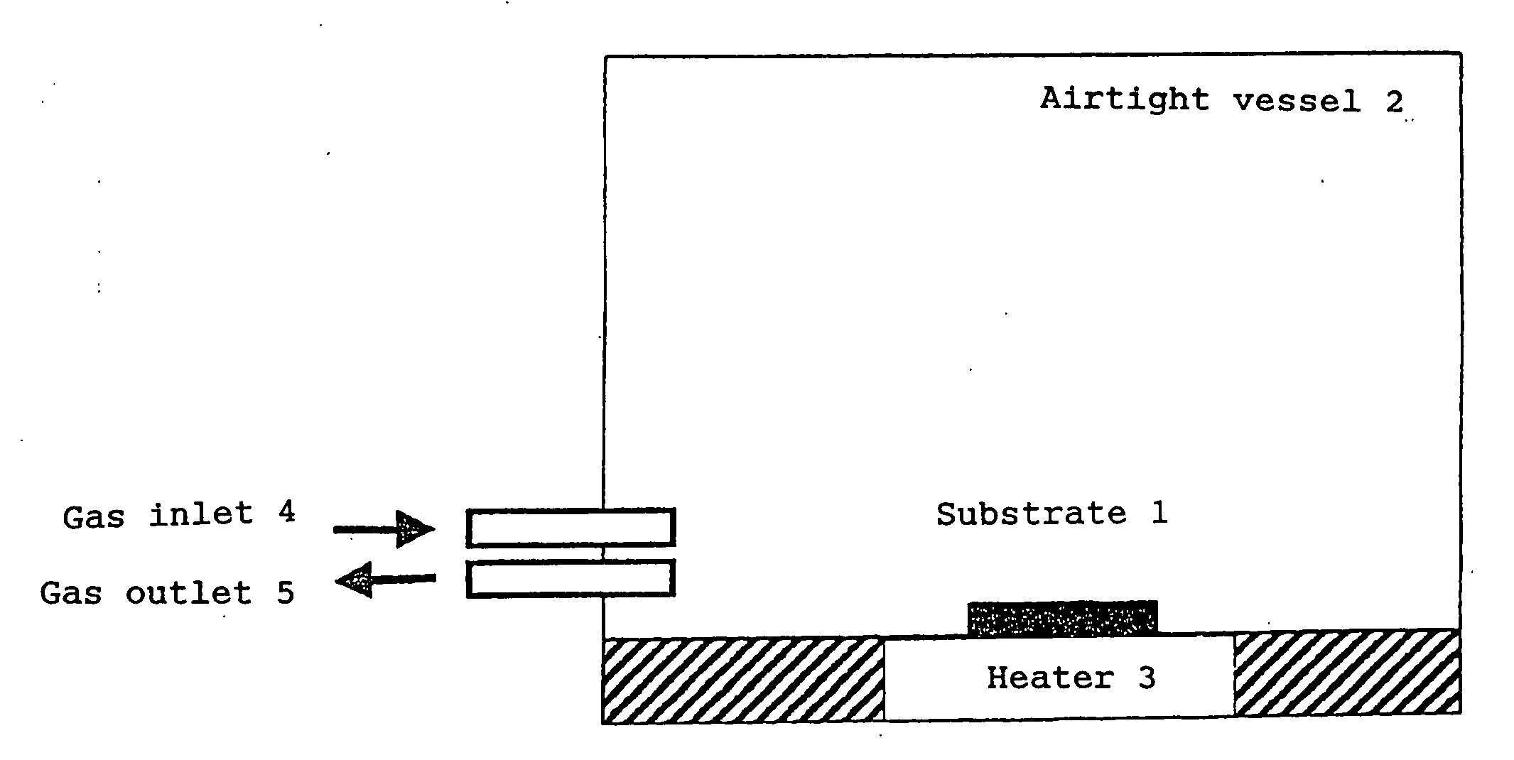
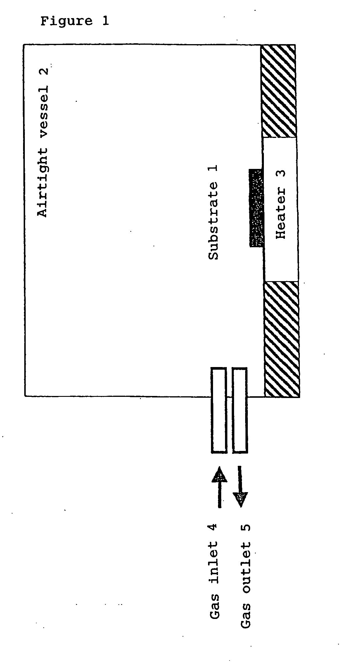
[0113] (Reduction / Baking Treatment in Vapor of Organic Compound)

[0114] A commercially available dispersion of copper ultra fine particles (brand name: independently dispersed ultra fine particle, Perfect copper made by Ulvac Materials, Inc.) was used, which is specifically a dispersion of copper nano-particles having a surface oxide film layer with an average particle diameter of 5 nm, containing 100 parts by mass of copper fine particles partially having an oxide film layer on the surface, 15 parts by mass of dodecylamine (the molecular weight of 185.36 and the boiling point of 248° C.) as an alkyl amine, and 75 parts by mass of mineral spirit as an organic solvent.

[0115] To 100 parts by mass of a dispersion of the copper ultra fine particles, 5 parts by mass of toluene was added, and then 100 parts by mass of methanol was added to precipitate the contained copper fine particles. With respect to 80 parts by mass of the copper fine particles, whi...

examples 1-5 to 1-11

AND COMPARATIVE EXAMPLE 1-4

[0120] (Reduction / Baking in Presence of Organic Compound Contained in Coated Layer)

[0121] At first, an aqueous dispersion containing copper ultra fine particles was prepared by a wet reductive reaction. After 30 g of copper sulfate was dissolving in 100 ml of distilled water, 100 g of diethanolamine was added as a reducing agent into the aqueous solution which was heated to 80° C. Subsequently, a wet reductive reaction was proceeded for eight hours while stirring was continued, and a dark brown aqueous dispersion containing formed copper fine particles was obtained. Acetone was added into the dispersion to remove diethanolamine and precipitate copper fine particles. The cleaning operation with the use of acetone was repeated three times to remove a remaining raw material, a by-product due to a reaction and impurities. The obtained copper fine particles had a surface oxide film layer partially on the surface, which is oxidized copper, and had the average p...

example 1-12

[0127] (Reduction / Baking Treatment in Vapor of Organic Compound)

[0128] A commercially available dispersion of copper ultra fine particles (brand name: independently dispersed ultra fine particle Perfectcopper, made by Ulvac Materials, Inc.) was used, which is a dispersion of copper nano-particles having partially an oxide film layer with an average particle diameter of 5 nm on the surface, specifically containing 100 parts by mass of copper fine particles, 15 parts by mass of dodecylamine (the molecular weight of 185.36 and the boiling point of 248° C.) for an alkyl amine, and 75 parts by mass of mineral spirit as an organic solvent.

[0129] To 100 parts by mass of a dispersion of the copper ultra fine particles, 5 parts by mass of toluene was added, and then 100 parts by mass of methanol was added to precipitate the contained copper fine particles. With respect to 80 parts by mass of the copper fine particles, which was collected by removing a supernatant liquid, and removing a rem...


PUM

PropertyMeasurementUnit
Temperatureaaaaaaaaaa
Lengthaaaaaaaaaa

Abstract

The present invention provides a process for forming a copper fine particle sintered product type of a fine-shaped electric conductor showing superior electroconductivity, which comprises steps of drawing a fine pattern with the use of a dispersion containing the copper fine particles having a surface oxide film layer, conducting a treatment for reducing the copper fine particles with the surface oxide film layer or copper oxide fine particles included in the pattern at a comparatively low temperature, and baking the resultant copper fine particles. Specifically, the process carries out the processes of; applying a dispersion containing the copper fine particles having the surface oxide film layer thereon or the copper oxide fine particles with an average particle diameter of 10 μm or smaller onto a substrate; and then performing a series of the heat treatment steps of heating the particles in the coated layer at temperature of 350° C. or lower under an atmosphere containing a vapor and a gas of a compound having reducibility to reduce the oxide film by a reduction reaction which used the compound having reducibility as a reducing agent, subsequently repeating a heat treatment combining an oxidizing treatment of a short time with a re-reducing treatment, and sintering the resultant copper fine particles with each other to form a layer of the sintered product.

Description

TECHNICAL FIELD [0001] The present invention relates to a process for forming a copper-based wiring pattern or a copper thin-film layer with an extremely thin film thickness, and more specifically relates to a process for forming a wiring pattern of a copper-sintered product with low impedance and an extremely fine shape fit for digital high-density wiring, or forming a copper thin-film layer with an extremely thin film-thickness, which comprises the steps of: drawing an ultra fine pattern or forming a thin-film coating layer by using a dispersion of copper fine particles with a surface oxide film layer or copper oxide fine particles, particularly, a dispersion of copper nano-particles with the surface oxide film layer or copper oxide nano-particles; conducting treatment for reducing copper fine particles with the surface oxide film layer or copper oxide fine particles, particularly, copper nano-particles with the surface oxide film layer or copper oxide nano-particles included in t...

Claims


Application Information

Patent Timeline
IPC IPC(8): C23C26/00B05D3/02H05K3/10
CPCH01B1/22H05K3/102H05K3/105H05K3/1283H05K2201/0257H05K2203/0315H05K2203/1131H05K2203/1157H05K2203/122H05K3/10B82Y40/00
Inventor ITOH, DAISUKEIZUMITANI, AKIHITOHATA, NORIAKIMATSUBA, YORISHIGE
Owner HARIMA CHEM INC
Learn More