Photomask blank, method for manufacturing photomask, and mask pattern formation method

a technology of photoresist film and mask pattern, which is applied in the field of photoresist film, method for manufacturing photoresist film, and mask pattern formation method, can solve the problems of increasing the demand for miniaturization of circuit pattern, and achieve satisfactory shape and dimensional accuracy, improve the adhesion of photoresist film, and maintain the stability of resist pattern

Active Publication Date: 2020-03-10
SHIN ETSU CHEM IND CO LTD
View PDF20 Cites 0 Cited by
  • Summary
  • Abstract
  • Description
  • Claims
  • Application Information

AI Technical Summary

Benefits of technology

[0029]The adhesion of a photoresist film is improved. When a fine resist pattern is formed in the photoresist film, the resist pattern is maintained stable without suffering degradation, collapse or stripping. When any underlying film is etched through the resist pattern, a pattern of satisfactory shape and dimensional accuracy is formed. As a result, a photomask having a mask pattern having a fine size at high accuracy is obtained.

Problems solved by technology

In the recent semiconductor processing technology, a challenge to higher integration of large-scale integrated circuits places an increasing demand for miniaturization of circuit patterns.

Method used


Image

  • Photomask blank, method for manufacturing photomask, and mask pattern formation method
  • Photomask blank, method for manufacturing photomask, and mask pattern formation method
  • Photomask blank, method for manufacturing photomask, and mask pattern formation method

Examples


example 1

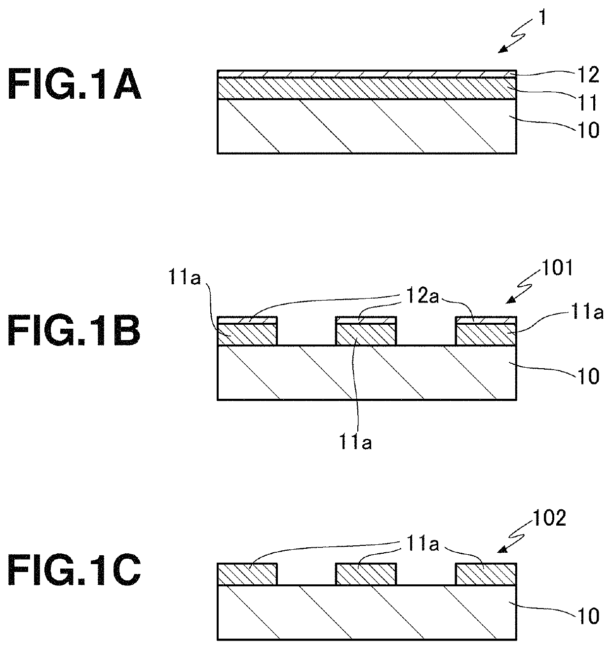
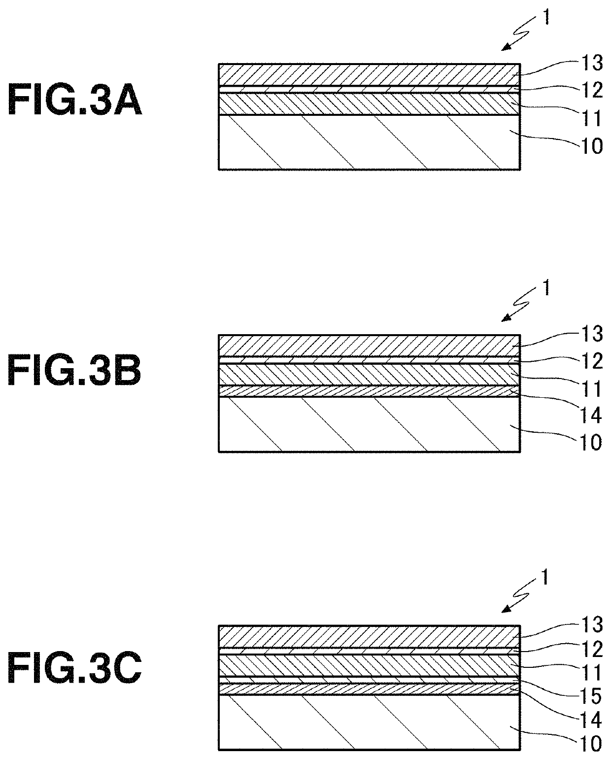
[0079]A phase shift film of MoSiON (75 nm thick) was deposited on a quartz substrate of 152 mm squares and ˜6 mm thick by sputtering. Deposition was carried out by using oxygen gas, nitrogen gas and argon gas as the sputtering gas, using two targets: MoSi2 target and Si target, and spinning the substrate at 30 rpm. The composition of the phase shift film was analyzed by ESCA using X-ray photoelectron spectrometer (K-Alpha by Thermo Fisher Scientific), finding Mo:Si:O:N=1:4:1:4 (atomic ratio).

[0080]Next, on the phase shift film, a light-shielding film consisting of two layers, a layer of CrN (30 nm thick) and a layer of CrON (20 nm thick) in order from the quartz substrate side was deposited as the first film by sputtering. Deposition was carried out by using nitrogen gas and argon gas for the CrN layer and oxygen gas, nitrogen gas and argon gas for the CrON layer as the sputtering gas, using metallic chromium as the target, and spinning the substrate at 30 rpm. The composition of th...


PUM

PropertyMeasurementUnit
wavelengthaaaaaaaaaa
thicknessaaaaaaaaaa
thicknessaaaaaaaaaa

Abstract

A photomask blank (1) having: a transparent substrate (10); a first film (11) etched by chlorine / oxygen-based dry etching and made of a material having resistance against fluorine-based dry etching; and a second film (12) formed adjacent to the first film and made of a material which comprises silicon and oxygen or silicon, oxygen, and nitrogen and has an Si—Si bond and which is substantially not etched by chlorine / oxygen-based dry etching, wherein: the photoresist adhesive performance is improved; the resist pattern is stably maintained without degrading, collapsing, or peeling even when a fine resist pattern is formed from a photoresist film; and an excellent shape and dimensional accuracy is obtained in regard to etching of a lower layer film in which the resist pattern is used.

Description

TECHNICAL FIELD[0001]This invention relates to photomask blanks from which photomasks for use in the microfabrication of semiconductor integrated circuits or the like are produced, a method for preparing a photomask, and a method for forming a mask pattern.BACKGROUND ART[0002]In the recent semiconductor processing technology, a challenge to higher integration of large-scale integrated circuits places an increasing demand for miniaturization of circuit patterns. There are increasing demands for further reduction in size of circuit-constructing wiring patterns and for miniaturization of contact hole patterns for cell-constructing inter-layer connections. As a consequence, in the manufacture of circuit pattern-written photomasks for use in the photolithography of forming such wiring patterns and contact hole patterns, a technique capable of accurately writing finer circuit patterns is needed to meet the miniaturization demand.[0003]In order to form a higher accuracy photomask pattern o...

Claims


Application Information

Patent Timeline
Patent Type & Authority Patents(United States)
IPC IPC(8): G06F1/00G03F1/32G03F1/46G03F1/38G03F1/58G03F1/80H01L21/033
CPCG03F1/38G03F1/46G03F1/80H01L21/0337G03F1/58G03F1/32G03F1/26
Inventor IRIE, SHIGEOYOSHII, TAKASHIMASUNAGA, KEIICHIINAZUKI, YUKIOKANEKO, HIDEOSAKURADA, TOYOHISA
Owner SHIN ETSU CHEM IND CO LTD
Why Eureka
Try Eureka