
Converse welding method of high power LED chip

A LED chip, high-power technology, applied in the direction of electrical components, electrical solid devices, circuits, etc., can solve problems such as thermal stress, lattice defects, shortening the life of LED chips, etc., to prolong life, improve thermal expansion matching performance, The effect of improving the luminous efficiency of the chip

Inactive Publication Date: 2007-05-30
CHONGQING UNIV OF POSTS & TELECOMM
View PDF0 Cites 13 Cited by
  • Summary
  • Abstract
  • Description
  • Claims
  • Application Information

AI Technical Summary

Problems solved by technology

However, the thermal expansion coefficient of gold is 14ppm / k. When gold bumps (gold balls) are soldered to LEDs, the thermal expansion mismatch rate is 42.85%, which will generate thermal stress, destroy the lattice of the LED chip, produce lattice defects, and form a recombination center , absorbing photons, reducing the luminous efficiency of the chip and shortening the life of the LED chip

Method used


Image

  • Converse welding method of high power LED chip
  • Converse welding method of high power LED chip

Examples


Embodiment Construction

[0019] The method of the present invention will be further described below in conjunction with the drawings, but it is not limited thereto.

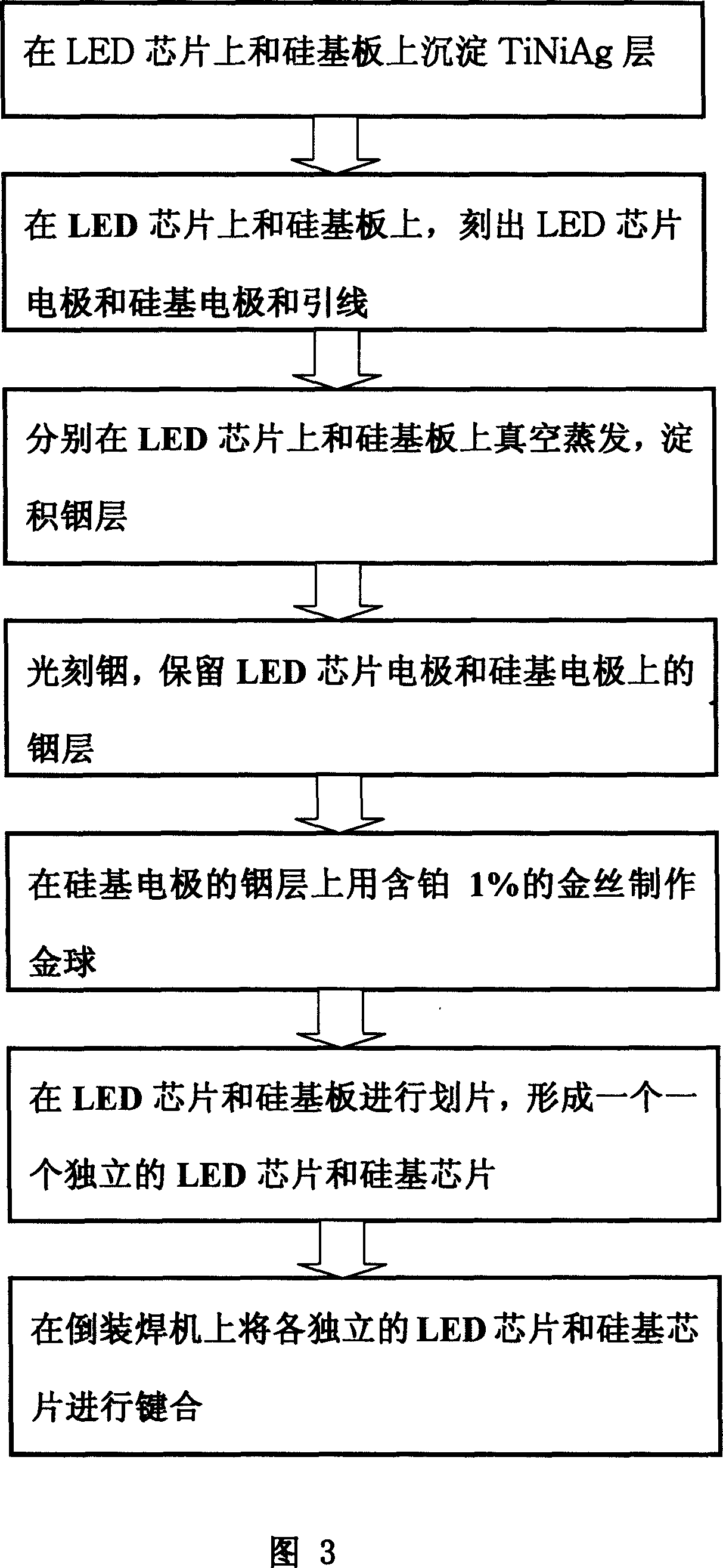
[0020] As shown in the figure, the present invention is to flip-chip the LED chip (including the sapphire substrate 6 and the GaN epitaxial layer 5 fabricated on the sapphire substrate 6) that emits light from the back side in a prefabricated fabric with multiple surge limiting and electrostatic Protect the circuit on the silicon substrate 11. The specific assembly and welding process is shown in Figure 3, including the following steps:

[0021] 1. The GaN epitaxial layer 5 fabricated on the LED chip sapphire substrate is metalized by a conventional integrated circuit vacuum coating method, and a TiNiAg (titanium nickel silver) layer 7 is formed on the surface, with titanium as the contact adhesion layer and nickel as The barrier layer, silver is used as a reflective conductive layer.

[0022] 2. Using conventional photolithography, the TiNi...


PUM


Abstract

This invention relates to one large power LED chip inverse weld method in micro electron technique, which comprises the following steps: depositing Tania layer on LED chip and metal indium on LED chip electrode; depositing Tania layer on silicon baseboard and indium on silicon base circuit board on LED chip electrode position to process gold ball; then welding the LED chip and silicon baseboard together to form indium to gold to cadmium structure with cadmium as expansion buffer.

Description

Technical field [0001] The invention relates to an LED (semiconductor light emitting diode) packaging method, in particular to a high-power LED chip assembly and welding method. Background technique [0002] LED devices are current-type devices. To make semiconductor light sources practical, high-power and high-brightness light-emitting LEDs must be developed. In the case of a certain conversion efficiency, in order to achieve high LED brightness, it is necessary to increase the current and light-emitting area, which will lead to a significant increase in LED power. With the increase of power, the junction temperature of the LED chip rises, reaching above 100°C, causing many problems during the operation of the LED chip, such as the temperature quenching effect, which causes the light efficiency of the LED chip and phosphor powder to decrease, the brightness decreases, and the work Color drift, device material deterioration, and yellowing of the encapsulating resin are caused in ...

Claims


Application Information

Patent Timeline
Patent Type & Authority Applications(China)
IPC IPC(8): H01L33/00H01L21/60
CPCH01L2224/16
Inventor 唐政维李秋俊关鸣蔡雪梅何小凡
Owner CHONGQING UNIV OF POSTS & TELECOMM
Learn More