


Quick Research
Generate reliable direction feasibility study reports for your R&D in just a few steps.

Technical Q&A
Discover and master advanced knowledge NOW. Basics, ideas, possibilities, all at once.

Find Solutions
As an expert in R&D theories, this can generate solutions to your technical problems instantly.

Evaluate Feasibility
Analyze your overall solution with one click, know your potential R&D risks in advance.

Monitor Landscape
Get weekly tech updates, stay abreast of the latest tech innovations and key insights.
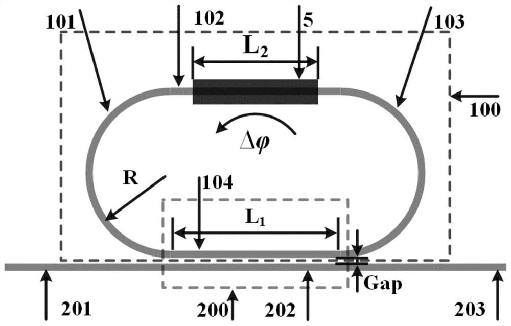
Runway type micro-ring optical switch based on silicon dioxide/polymer mixed waveguide and preparation method of runway type micro-ring optical switch
A silicon dioxide and polymer technology, applied in optical waveguide, optical waveguide coupling, optics, etc., can solve the problems of large device size, difficulty in large-scale integration, and only tens of milliwatts, etc., to achieve compact end face size, The effect of low processing cost and fast response
- Summary
- Abstract
- Description
- Claims
- Application Information
AI Technical Summary
Problems solved by technology
Method used
Image

Examples
Embodiment 1
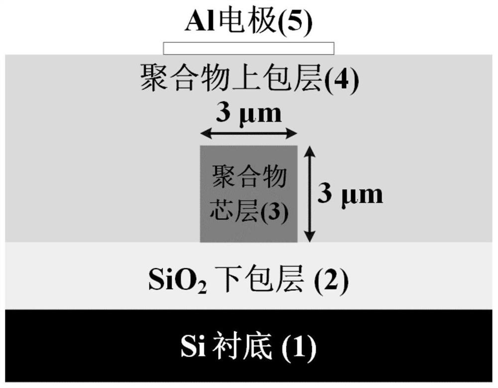
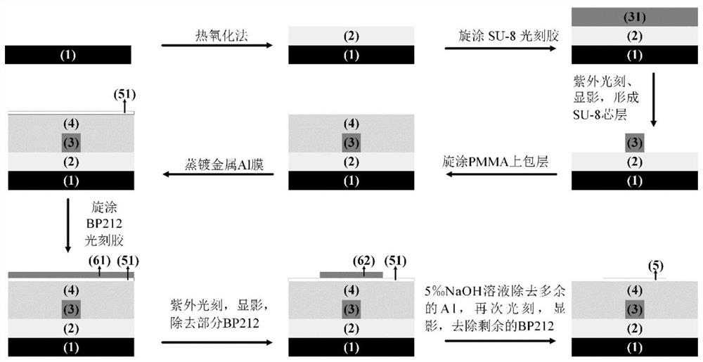
[0034] as attached figure 1 Shown is a schematic cross-sectional view of the polymer / silica hybrid waveguide, from bottom to top, consisting of Si substrate (1), SiO2 It consists of a lower cladding layer (2), a polymer core layer (3), a polymer upper cladding layer (4) and a metal electrode (5). The SiO 2 The lower cladding layer (2) can be grown by thermal oxidation or (Plasma Enhanced Chemical Vapor Deposition, PECVD) deposition method. In this embodiment, thermal oxidation is used to grow SiO 2 , the refractive index is 1.4456. The polymer core layer (3) can use a polymer material with a negative thermo-optic coefficient, including SU-8 2002, SU-8 2005, EpoCore, etc. In this embodiment, the SU-8 2002 material is used as the polymer material The material of the core layer (3) has a refractive index of 1.573. The polymer upper cladding (4) material can be polymethyl methacrylate (PMMA), polyethylene (PE), polyester (PET), polystyrene (PS), EpoClad, etc., in this embodimen...
PUM
| Property | Measurement | Unit |
|---|---|---|
| Thickness | aaaaa | aaaaa |
| Width | aaaaa | aaaaa |
| Thickness | aaaaa | aaaaa |
Abstract
Description
Claims
Application Information
 - R&D Engineer
- R&D Manager
- IP Professional
- Industry Leading Data Capabilities
- Powerful AI technology
- Patent DNA Extraction
Browse by: Latest US Patents, China's latest patents, Technical Efficacy Thesaurus, Application Domain, Technology Topic, Popular Technical Reports.
© 2024 PatSnap. All rights reserved.Legal|Privacy policy|Modern Slavery Act Transparency Statement|Sitemap|About US| Contact US: help@patsnap.com