


Quick Research
Generate reliable direction feasibility study reports for your R&D in just a few steps.

Technical Q&A
Discover and master advanced knowledge NOW. Basics, ideas, possibilities, all at once.

Find Solutions
As an expert in R&D theories, this can generate solutions to your technical problems instantly.

Evaluate Feasibility
Analyze your overall solution with one click, know your potential R&D risks in advance.

Monitor Landscape
Get weekly tech updates, stay abreast of the latest tech innovations and key insights.
Ceramic surface metallization method and metallized ceramic
A ceramic surface and metallization technology, which is applied in the field of metallized ceramics and ceramic surface metallization, can solve problems such as unstable performance of power devices, complicated process, and large copper foil thickness, and achieves the avoidance of oxygen residues, advanced preparation methods, cost-effective preparation
- Summary
- Abstract
- Description
- Claims
- Application Information
AI Technical Summary
Problems solved by technology
Method used
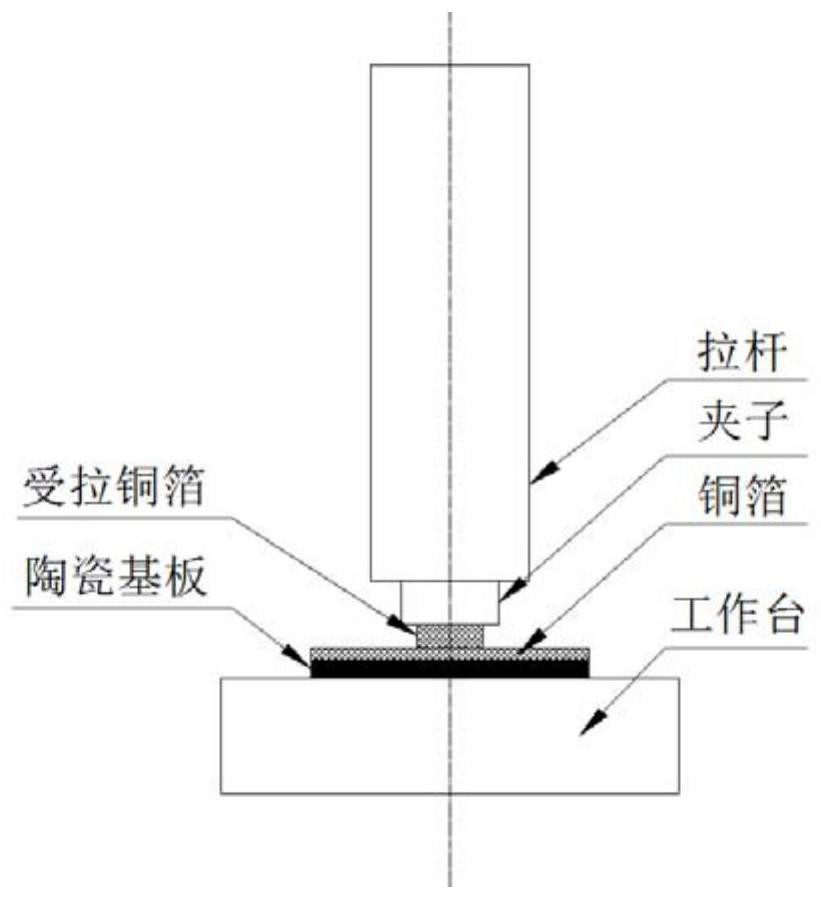
Image


Examples
Embodiment 1
[0089] This embodiment provides a method for metallizing ceramic surfaces and metallized ceramics, the steps are as follows:
[0090] S1. Use the laser beam to irradiate the ceramic substrate. The parameters of the laser beam are: laser pulse width 2.4t / ms, laser frequency 4.5f / Hz, laser scanning speed 330V / (mm*min -1 ), writing a circuit pattern area on the ceramic substrate;
[0091] S2. Immerse the irradiated ceramic substrate in a copper plating solution for electroless copper plating, and grow a seed copper layer with a thickness of 1000 nm on the circuit pattern area; wherein, the copper plating solution includes water and the following concentration components: copper sulfate 0.8g*L -1 , Formaldehyde 0.5g*L -1 , sodium potassium tartrate 5g*L -1 、EDTA2NA 5g*L -1 , Sodium hydroxide 2.5g*L -1 .
[0092] S3, on the seed copper layer, lay liquid solder CuNi 12 Ti 35 , and then lay a copper foil with a thickness of 0.8mm, and braze for 30min at a vacuum of 300Pa and ...
Embodiment 2
[0095] This embodiment provides a method for metallizing ceramic surfaces and metallized ceramics, which are different from the process parameters in Embodiment 1, and the steps are as follows:
[0096] S1. Use the laser beam to irradiate the ceramic substrate. The parameters of the laser beam are: laser pulse width 2.3t / ms, laser frequency 5f / Hz, laser scanning speed 320V / (mm*min -1 ), writing a circuit pattern area on the ceramic substrate;
[0097] S2. Immerse the irradiated ceramic substrate in a copper plating solution for electroless copper plating, and grow a seed copper layer with a thickness of 1100 nm on the circuit pattern area; wherein, the copper plating solution includes water and the following concentration components: chloride Copper 1g*L -1 , Formaldehyde 0.4g*L -1 , sodium potassium tartrate 5g*L -1 、EDTA2NA 5g*L -1 , Sodium hydroxide 3g*L -1 .
[0098] S3, on the seed copper layer, lay liquid solder CuNi 12 Ti 35 , and then lay a copper foil with a thi...
Embodiment 3
[0101] This embodiment provides a method for metallizing ceramic surfaces and metallized ceramics, which are different from the process parameters in Embodiment 1, and the steps are as follows:
[0102] S1. Use the laser beam to irradiate the ceramic substrate. The parameters of the laser beam are: laser pulse width 2.4t / ms, laser frequency 4.5f / Hz, laser scanning speed 330V / (mm*min -1 ), writing a circuit pattern area on the ceramic substrate;
[0103] S2. Immerse the irradiated ceramic substrate in a copper plating solution for electroless copper plating, and grow a seed copper layer with a thickness of 1200 nm on the circuit pattern area; wherein, the copper plating solution includes water and the following concentration components: copper sulfate 0.8g*L -1 , Formaldehyde 0.5g*L -1 , sodium potassium tartrate 5g*L -1 、EDTA2NA 5g*L -1 , Sodium hydroxide 2.5g*L -1 .
[0104] S3, on the seed copper layer, lay liquid solder CuNi 12 Ti 35 , and then lay a copper foil wit...
PUM
| Property | Measurement | Unit |
|---|---|---|
| thickness | aaaaa | aaaaa |
| thickness | aaaaa | aaaaa |
Abstract
Description
Claims
Application Information
 - R&D Engineer
- R&D Manager
- IP Professional
- Industry Leading Data Capabilities
- Powerful AI technology
- Patent DNA Extraction
Browse by: Latest US Patents, China's latest patents, Technical Efficacy Thesaurus, Application Domain, Technology Topic, Popular Technical Reports.
© 2024 PatSnap. All rights reserved.Legal|Privacy policy|Modern Slavery Act Transparency Statement|Sitemap|About US| Contact US: help@patsnap.com