Method for preparing GaN-based electronic device

A technology for electronic devices and microwave devices is applied in the field of preparing GaN-based electronic devices and semiconductor devices. The effect of reducing RF loss and ensuring crystal quality

Pending Publication Date: 2022-01-04
SUZHOU INST OF NANO TECH & NANO BIONICS CHINESE ACEDEMY OF SCI
View PDF0 Cites 1 Cited by
  • Summary
  • Abstract
  • Description
  • Claims
  • Application Information

AI Technical Summary

Problems solved by technology

However, GaN heteroepitaxy based on high-resistance Si substrates has its own unique problems: on the one hand, due to the band difference between the epitaxial layer and the Si substrate, there may be an electronically conductive layer at the interface of the epitaxial layer / Si substrate; on the other hand, During the epitaxial growth process, due to thermal driving, group III metal atoms (such as Al atoms, Ga atoms) inevitably diffuse to the Si substrate and become acceptor impurities, which may form a p-type conductive layer
Some researchers proposed a low-temperature AlN nucleation layer growth technology, trying to suppress the thermal diffusion of Al atoms through the regulation of epitaxial growth parameters, and then suppress the p-type interface conductive layer, which can suppress the thermal diffusion of Al atoms to a certain extent, thereby suppressing the p-type parasitic Conductive layer, however, this method is at the cost of sacrificing the crystal quality, which will increase the dislocations and defects in the AlN nucleation layer, so the AlN nucleation layer itself will show a certain conductivity, which will increase the RF loss of the device
Another researcher proposed a diffusion barrier layer (Diffusion Barrier) technology, by first epitaxially growing SiN on a Si substrate x , to prevent the thermal diffusion of Al atoms during the subsequent epitaxial growth of the AlN nucleation layer, thereby inhibiting the interfacial conductive layer. This method can also inhibit the thermal diffusion of Al atoms, but the quality of AlN crystals will also decrease, especially threading dislocations will increase. The increase of the corresponding leakage channel will also increase the RF loss of the device
Some researchers also proposed the method of ion implantation after epitaxial growth, that is, after the epitaxial growth of a certain thickness of the epitaxial layer, the use of ion implantation to physically destroy the interface conductive layer, and then complete the growth of the entire structure of the radio frequency microwave device through secondary epitaxy. Through physical bombardment, the interface conductive layer can be completely destroyed, but due to the limitation of implanted ion depth, it is necessary to perform ion implantation after growing a thin epitaxial layer (such as growing a certain thickness of AlN nucleation layer) on the silicon substrate. Then the whole structure is grown by secondary epitaxy. Therefore, the problem of the secondary epitaxy interface is inevitable. In fact, there are many problems such as impurity incorporation and carbon and oxygen contamination at the secondary epitaxy interface, which will introduce the problem of the interface conductive layer again. As a result, the RF loss of the device increases

Method used


Image

  • Method for preparing GaN-based electronic device
  • Method for preparing GaN-based electronic device
  • Method for preparing GaN-based electronic device

Examples


Embodiment 1

[0089] Embodiment 1: A preparation process of a silicon-based GaN radio frequency microwave device comprises the following steps:

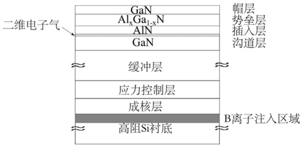
[0090] 1) High resistance Si substrate (resistivity>10 4 Ω cm) surface doping. Using boron ion implantation, the implantation energy is 1keV, and the implantation dose is 1×10 6 / cm 2 .

[0091] 2) B ion activation. The rapid annealing process is adopted, the annealing temperature is 1000°C, the annealing time is 30s, and the annealing atmosphere is nitrogen.

[0092] 3) AlN nucleation layer growth. Using MOCVD equipment, heat treatment at a temperature of 1100°C and hydrogen atmosphere for 5 minutes to remove the surface oxide layer; then lower the temperature to 1080°C, feed Al source to pre-spread Al; finally control the pressure of the reaction chamber to 10mbar, the flow rate of TMAl to 20sccm, and the flow rate of ammonia gas to 1slm , to grow an AlN nucleation layer with a thickness of 10nm.

[0093] 4) Gradual Al composition stress ...

Embodiment 2

[0101] Embodiment 2: A preparation process of a silicon-based GaN radio frequency microwave device comprises the following steps:

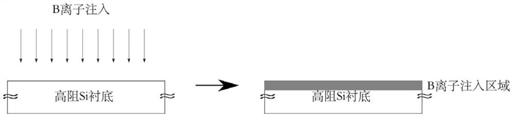
[0102] 1) High resistance Si substrate (resistivity>10 4 Ω cm) surface doping. Boron ion implantation is adopted, the implantation energy is 1MeV, and the implantation dose is 1×10 20 / cm 2 ,Such as figure 1 shown.

[0103] 2) B ion activation. The rapid annealing process is adopted, the annealing temperature is 700°C, the annealing time is 30min, and the annealing atmosphere is nitrogen.

[0104] 3) AlN nucleation layer growth. Using MOCVD equipment, heat treatment at a temperature of 1050°C and hydrogen atmosphere for 5 minutes to remove the surface oxide layer; then lower the temperature to 1000°C, feed Al source to pre-spread Al; finally control the pressure of the reaction chamber to 200mbar, the flow rate of TMAl to 200sccm, and the flow rate of ammonia gas to 20slm , to grow an AlN nucleation layer with a thickness of 1000nm.

[010...

Embodiment 3

[0112] Embodiment 3: A preparation process of a silicon-based GaN radio frequency microwave device comprises the following steps:

[0113] 1) High resistance Si substrate (resistivity>10 4 Ω cm) surface doping. Phosphorus (P) ion implantation is adopted, the implantation energy is 0.5MeV, and the implantation dose is 5×10 10 / cm 2 .

[0114] 2) P ion activation. The rapid annealing process is adopted, the annealing temperature is 900°C, the annealing time is 1min, and the annealing atmosphere is nitrogen.

[0115] 3) AlN nucleation layer growth. Using MOCVD equipment, heat treatment at a temperature of 1100°C and hydrogen atmosphere for 5 minutes to remove the surface oxide layer; then lower the temperature to 1000°C, feed Al source to pre-spread Al; finally control the pressure of the reaction chamber to 100mbar, the flow rate of TMAl to 100sccm, and the flow rate of ammonia gas to 10slm , to grow an AlN nucleation layer with a thickness of 500nm.

[0116] 4) Gradual A...


PUM

PropertyMeasurementUnit
thicknessaaaaaaaaaa
thicknessaaaaaaaaaa
electrical resistivityaaaaaaaaaa

Abstract

The invention discloses a method for preparing a GaN-based electronic device. The method comprises the steps: carrying out doping treatment on the surface of a high-resistance substrate to make any one or more of vacant sites, gap sites and replacement sites on the surface of the high-resistance substrate be occupied by doping ions and / or doping atoms, so that external Al atoms and / or Ga atoms can be prevented from diffusing into the high-resistance substrate or parasitic conduction is inhibited by using a compensation mechanism; then growing an epitaxial structure containing Al atoms and / or Ga atoms on the surface of the high-resistance substrate; and manufacturing a GaN-based electronic device based on the epitaxial structure. The invention also discloses a GaN-based electronic device prepared by using the method. According to the invention, the manufacturing method of the GaN-based electronic device is simple and effective, the crystal quality of the epitaxial layer can be guaranteed, and the problems of secondary epitaxial interface impurity contamination, low production efficiency and the like are solved, so that the GaN-based radio frequency microwave device epitaxial wafer with low radio frequency loss and high performance can be manufactured.

Description

technical field [0001] The invention relates to a method for preparing a semiconductor device, in particular to a method for preparing a GaN-based electronic device, and belongs to the technical field of semiconductors. Background technique [0002] Gallium nitride (GaN), as a representative of the third-generation wide bandgap semiconductor, has the advantages of large bandgap width, high electron mobility and breakdown field strength. The device power density is higher than that of silicon (Si), gallium arsenide ( GaAs) more than 10 times the power density. Due to its excellent characteristics such as high frequency, high power, high efficiency, high temperature resistance, and radiation resistance, it can be widely used in 5G-oriented RF microwave frequency band civil communication base stations, mobile phone RF chips, and cutting-edge military equipment. Therefore, it has become a new generation of solid-state RF The frontier hot spot of microwave device and material re...

Claims


Application Information

Patent Timeline
Patent Type & Authority Applications(China)
IPC IPC(8): H01L21/265H01L29/778H01L21/335
CPCH01L21/26513H01L29/7787H01L29/66462
Inventor 孙钱周宇刘建勋孙秀建詹晓宁高宏伟钟耀宗
Owner SUZHOU INST OF NANO TECH & NANO BIONICS CHINESE ACEDEMY OF SCI
Why Eureka
Try Eureka