Electrode design and cell interconnection method of heterojunction solar cell with double-sided power generation
A technology for designing solar cells and electrodes, applied in the field of solar cells, can solve the problems of poor adhesion and large consumption of silver paste in heterojunction solar cells, and achieve the effect of solving poor adhesion characteristics and saving consumption of silver paste
- Summary
- Abstract
- Description
- Claims
- Application Information
AI Technical Summary
Problems solved by technology
Method used
Image
Examples
Embodiment 1
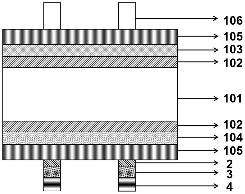
[0060] This embodiment describes in detail the electrode design method of a heterojunction solar cell that generates electricity on both sides. see figure 1 , wherein, 101-106 constitute the heterojunction solar cell substrate (1), and 2-4 constitute the solar cell backlight electrodes.
[0061] The process steps are:
[0062] a. Clean the N-type monocrystalline silicon chip (101) with the RCA method, and then corrode the silicon chip with an alkaline solution to make texture;
[0063] b. Depositing an intrinsic amorphous silicon layer (102) by PECVD on both sides of the silicon wafer with a thickness of 5nm;
[0064] c. Depositing an n-type amorphous silicon layer (103) with a thickness of 10 nm by PECVD;
[0065] d. Depositing a p-type amorphous silicon layer (104) with a thickness of 10 nm by PECVD method;
[0066] e. on the n-type amorphous silicon layer (103) and the p-type amorphous silicon layer (104), deposit a transparent conductive film IWO (105) with a thickness...
Embodiment 2
[0071] This example specifically describes the interconnection method of double-sided heterojunction solar cells. On the basis of the aforementioned preparation method, the working process and technical parameters are further limited to realize the interconnection technology. Please refer to figure 1 and figure 2 :
[0072] a. Prepare two double-sided heterojunction solar cells by the method of Example 1;
[0073] b. Fix the conductive grid line (5) on the electrode on the backlight surface of the heterojunction solar cell, which is directly connected to the welding layer (4) on the metal grid line on the light incident surface of another adjacent heterojunction solar cell; The conductive grid wires are copper or aluminum with a diameter of 1-50 μm, and the number of conductive grid wires on each heterojunction solar cell is ≥ 56; the fixing method is welding or hot pressing.
[0074] In this embodiment, combined with the electrode design method in Embodiment 1, conductive ...
PUM
| Property | Measurement | Unit |
|---|---|---|
| thickness | aaaaa | aaaaa |
| thickness | aaaaa | aaaaa |
| electrical conductivity | aaaaa | aaaaa |
Abstract
Description
Claims
Application Information
 - R&D
- Intellectual Property
- Life Sciences
- Materials
- Tech Scout
- Unparalleled Data Quality
- Higher Quality Content
- 60% Fewer Hallucinations
Browse by: Latest US Patents, China's latest patents, Technical Efficacy Thesaurus, Application Domain, Technology Topic, Popular Technical Reports.
© 2025 PatSnap. All rights reserved.Legal|Privacy policy|Modern Slavery Act Transparency Statement|Sitemap|About US| Contact US: help@patsnap.com


