High-reliability three-dimensional heterogeneous integrated radio frequency analog-digital integrated microsystem

An integrated radio frequency, analog and digital technology, which is applied in the field of highly reliable three-dimensional heterogeneous integrated radio frequency analog and digital integrated microsystems, can solve the problems of high shell cost, complex overall design, and many wiring layers, and reduce bonding Refers to the effect of area, reducing the number of wiring layers, and reducing the package volume

Active Publication Date: 2021-06-04
NO 55 INST CHINA ELECTRONIC SCI & TECHNOLOGYGROUP CO LTD
View PDF3 Cites 0 Cited by
  • Summary
  • Abstract
  • Description
  • Claims
  • Application Information

AI Technical Summary

Problems solved by technology

[0006] The traditional high-reliability airtight ceramic package RF microsystem uses a multi-step multi-cavity multi-layer wiring integrated ceramic shell package. The ceramic shell is used as both the package body and the wiring layer. Layer step bonding refers to design, multi-layer high-speed wiring and multi-cavity structure design. Due to the limited wiring accuracy of ceramic materials, the number of wiring layers is large, the overall design is complex, the process is difficult to realize, the processing cycle is long, and the production yield is low. The cost of the shell is high, and it is difficult to promote it on a large scale in engineering. In addition, no matter whether the circuit design needs to be modified or the structure of the shell needs to be modified, the ceramic shell needs to be redesigned and processed. The iteration cycle is too long, which is not conducive to the rapid launch of products and seize market opportunities.

Method used


Image

  • High-reliability three-dimensional heterogeneous integrated radio frequency analog-digital integrated microsystem
  • High-reliability three-dimensional heterogeneous integrated radio frequency analog-digital integrated microsystem
  • High-reliability three-dimensional heterogeneous integrated radio frequency analog-digital integrated microsystem

Examples


Embodiment

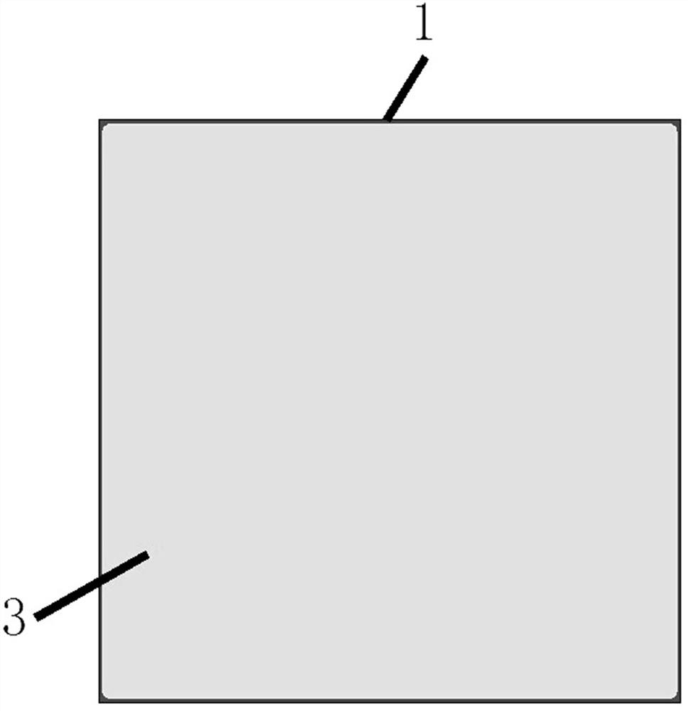
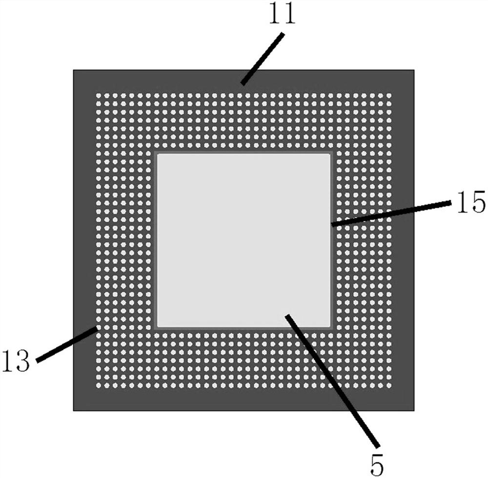
[0048] combine Figure 1 ~ Figure 3 , the RF analog-digital integrated microsystem provided by the present invention is composed of 15 parts, including a ceramic base 1, a radio frequency frame 2, a radio frequency cover 3, a digital-analog frame 4, a digital-analog cover 5, a radio-frequency substrate 6, a digital Mold substrate 7 , wire bonding 8 , flip chip 9 , SMT 10 , polymer base 11 , inner BGA solder ball 12 , outer BGA solder ball 13 , inner underfill 14 , and outer underfill 15 .

[0049] like Figure 4 , Figure 5 As shown, the radio frequency analog-digital integrated microsystem of the present invention adopts a four-layer high-density radio frequency substrate and a ten-layer high-density digital-analog substrate as the wiring medium, and fully utilizes the organic packaging substrate / silicon-based adapter board / glass-based adapter board. High-density interconnection capability realizes signal interconnection within the circuit, which can replace the traditional...


PUM


Abstract

The invention relates to a high-reliability three-dimensional heterogeneous integrated radio frequency analog-digital integrated microsystem. Three-dimensional heterogeneous integration is realized through three-level POP stacking, a high-density radio frequency substrate and a high-density digital-analog substrate are stacked in a ceramic base through internal BGA solder balls, the high-density substrate is used as a wiring medium, the ceramic base serves as an airtight packaging body and a signal fan-out medium, after the ceramic base is sealed, POP stacking is conducted on the ceramic base and a polymer base, a gap is filled with underfill glue, the polymer base conducts vertical signal transmission, and a final complete packaging body structure is formed. A traditional multi-step multi-cavity multi-layer wiring integrated ceramic tube shell packaging mode is replaced, packaging design is greatly simplified, meanwhile, the problems that when a traditional ceramic tube shell and a PCB are directly welded, due to the fact that thermal stress generated by large material thermal expansion coefficient difference is large, welding balls and bonding pads lose efficacy are solved, the process difficulty is lowered, and meanwhile, high-density integration and high reliability are realized.

Description

technical field [0001] The invention is a highly reliable three-dimensional heterogeneous integrated radio frequency analog-digital integrated microsystem, which belongs to the technical field of microelectronic packaging. Background technique [0002] Moore's Law is approaching the physical limit, but in the future, electronic information systems will continue to develop towards higher integration, higher performance, and higher operating frequency. Traditional integrated packaging technology is gradually difficult to meet the requirements of new system integration. The future technology development trend will be to continue Moore's Law and to combine Moore's Law, through three-dimensional heterogeneous heterogeneous integration, to achieve higher value systems - microsystems. Microsystem integration technology is the main means to achieve higher integration, higher performance, and higher operating frequency requirements through the integration of heterogeneous and heterog...

Claims


Application Information

Patent Timeline
IPC IPC(8): H01L23/538H01L23/08
CPCH01L23/5385H01L23/5386H01L23/08Y02D30/70
Inventor 杨进周明邵登云
Owner NO 55 INST CHINA ELECTRONIC SCI & TECHNOLOGYGROUP CO LTD
Why Eureka
Try Eureka